


Quick Research
Generate reliable direction feasibility study reports for your R&D in just a few steps.

Technical Q&A
Discover and master advanced knowledge NOW. Basics, ideas, possibilities, all at once.

Find Solutions
As an expert in R&D theories, this can generate solutions to your technical problems instantly.

Evaluate Feasibility
Analyze your overall solution with one click, know your potential R&D risks in advance.

Monitor Landscape
Get weekly tech updates, stay abreast of the latest tech innovations and key insights.
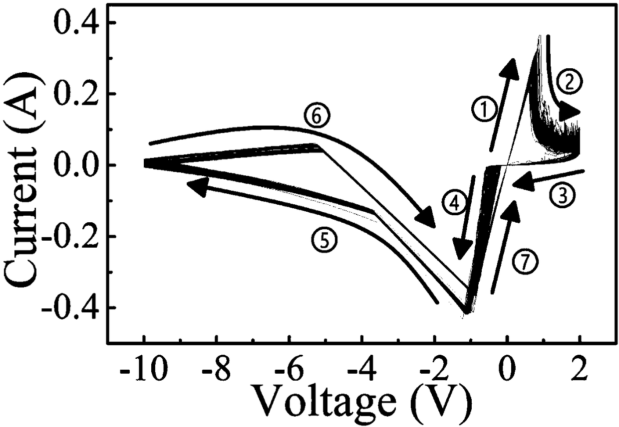
Preparation method for memory resistance and negative differential effect stabilization coexistence device at room temperature
A negative differential, room temperature technology, applied in electric solid devices, semiconductor devices, electrical components, etc., can solve problems such as restricting use value, and achieve the effects of low cost, good application prospects, and simple device structure
- Summary
- Abstract
- Description
- Claims
- Application Information
AI Technical Summary
Problems solved by technology
Method used
Image

Examples
Embodiment 1
[0029] A method for preparing a stable coexistence device of memristor and negative differential effect at room temperature, comprising the following steps:
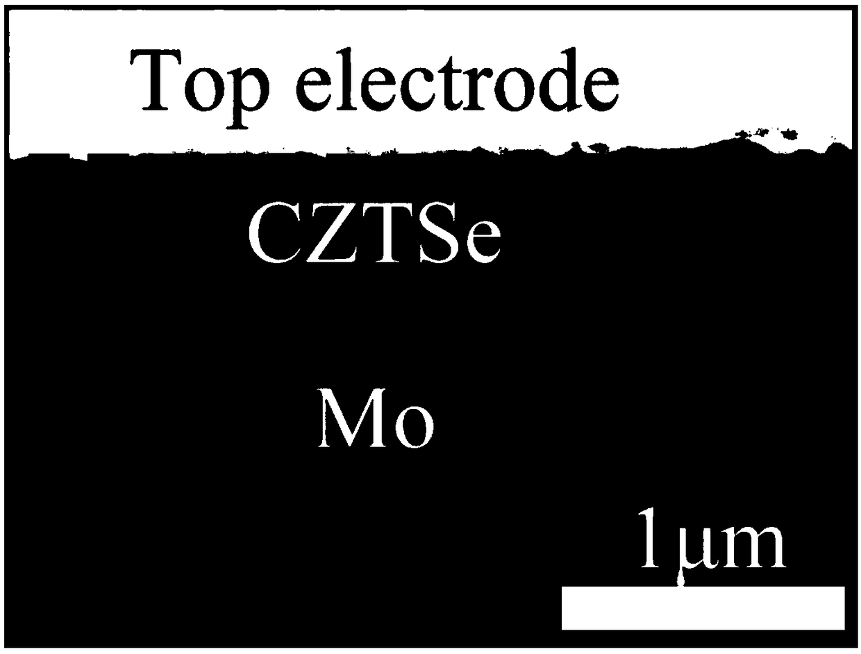
[0030]S1: Cleaning the substrate: Put the substrate into potassium dichromate solution, acetone, and deionized water alcohol in order to sonicate for 15 minutes respectively, clean and dry the substrate, and put it into the magnetron sputtering chamber for later use;
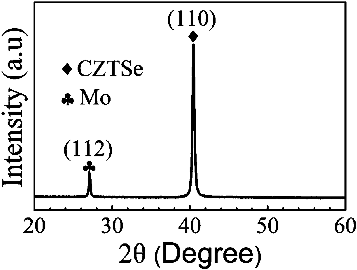
[0031] S2: Pre-sputtering: Mounting Cu on the magnetron sputtering target gun 2 ZnSnSe 4 Compound target material, the atomic ratio of Cu, Zn, Sn, Se is 2:1:1:4, the purity of the target material is 99%, the magnetron sputtering chamber is evacuated and then argon gas is introduced, and the substrate temperature is 200 ℃, set the distance from the target gun to the substrate to 10 cm, and pump the background vacuum of the sputtering chamber to less than 1x10 -3 Pa, the argon gas with a purity of 99.999% is introduced as the working gas, the baffle covers...
Embodiment 2
[0039] A method for preparing a stable coexistence device of memristor and negative differential effect at room temperature, comprising the following steps:
[0040] S1: Cleaning the substrate: Put the substrate into potassium dichromate solution, acetone, and deionized water alcohol in order to sonicate for 15 minutes respectively, clean and dry the substrate, and put it into the magnetron sputtering chamber for later use;
[0041] S2: Pre-sputtering: Mounting Cu on the magnetron sputtering target gun 2 ZnSnSe 4 Compound target material, the atomic ratio of Cu, Zn, Sn, Se is 2:1:1:4, the purity of the target material is 99%, the magnetron sputtering chamber is evacuated and then argon gas is introduced, and the substrate temperature is 200 ℃, set the distance from the target gun to the substrate to 10 cm, and pump the background vacuum of the sputtering chamber to less than 1x10 -3 Pa, the argon gas with a purity of 99.999% is introduced as the working gas, the baffle cover...
Embodiment 3
[0047] A method for preparing a stable coexistence device of memristor and negative differential effect at room temperature, comprising the following steps:
[0048] S1: Cleaning the substrate: Put the substrate into potassium dichromate solution, acetone, and deionized water alcohol in order to sonicate for 15 minutes respectively, clean and dry the substrate, and put it into the magnetron sputtering chamber for later use;
[0049] S2: Pre-sputtering: Mounting Cu on the magnetron sputtering target gun 2 ZnSnSe 4 Compound target material, the atomic ratio of Cu, Zn, Sn, Se is 2:1:1:4, the purity of the target material is 99%, the magnetron sputtering chamber is evacuated and then argon gas is introduced, and the substrate temperature is 300 ℃, set the distance from the target gun to the substrate as 12 cm, and pump the background vacuum of the sputtering chamber to less than 1x10 -3 Pa, introduce argon with a purity of 99.999% as the working gas, cover the substrate with the...
PUM
| Property | Measurement | Unit |
|---|---|---|
| Thickness | aaaaa | aaaaa |
| Thickness | aaaaa | aaaaa |
Abstract
Description
Claims
Application Information
 - R&D Engineer
- R&D Manager
- IP Professional
- Industry Leading Data Capabilities
- Powerful AI technology
- Patent DNA Extraction
Browse by: Latest US Patents, China's latest patents, Technical Efficacy Thesaurus, Application Domain, Technology Topic, Popular Technical Reports.
© 2024 PatSnap. All rights reserved.Legal|Privacy policy|Modern Slavery Act Transparency Statement|Sitemap|About US| Contact US: help@patsnap.com