


Quick Research
Generate reliable direction feasibility study reports for your R&D in just a few steps.

Technical Q&A
Discover and master advanced knowledge NOW. Basics, ideas, possibilities, all at once.

Find Solutions
As an expert in R&D theories, this can generate solutions to your technical problems instantly.

Evaluate Feasibility
Analyze your overall solution with one click, know your potential R&D risks in advance.

Monitor Landscape
Get weekly tech updates, stay abreast of the latest tech innovations and key insights.
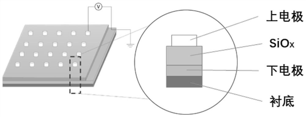
Silicon oxide-based memristor based on solution method as well as preparation method and application of silicon oxide-based memristor
A silicon oxide-based, memristor technology, applied in electrical components and other directions, can solve the problems of poor bonding between electrodes, insufficient compactness, holes, etc., and achieve the effects of low equipment requirements, good adhesion, and simple preparation process.
- Summary
- Abstract
- Description
- Claims
- Application Information
AI Technical Summary
Problems solved by technology
Method used
Image

Examples
Embodiment 1
[0053] The preparation method of the silicon oxide-based memristor in this embodiment is as follows: firstly, the lower electrode is prepared on the glass substrate; then the lower electrode is solidified and transformed by PHPS to prepare a silicon oxide film as the intermediate dielectric layer; finally, the upper electrode is prepared on the silicon oxide . details as follows:
[0054] 1) First, wash the surface of the glass sheet with detergent to remove stains; then use ethanol, acetone, and deionized water to ultrasonically clean for 30 minutes, and finally dry the surface with nitrogen to obtain a substrate with a clean surface. Au lower electrode layer was prepared on the substrate with a thickness of 50nm.
[0055] 2) Dilute perhydropolysilazane (PHPS) to 3% (mass fraction) with dibutyl ether, add 0.2% N,N-dimethylacetamide as a catalyst, oscillate and mix evenly through a high-speed oscillating disperser .
[0056] 3) After passing the solution prepared in step 2)...
Embodiment 2
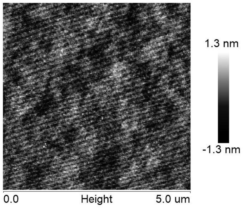
[0062] Adopt the preparation method of memristor in embodiment 1, but in SiO x During the preparation of the dielectric layer, damp heat is used for curing, as follows: the lower electrode / glass sheet coated with the PHPS film obtained in step 3) is placed in a constant temperature and humidity box at a temperature of 180°C and a humidity of 50%, and the holding time is 1.5h. That is, SiO x Dielectric layer, the resulting memristor structure is Ag / SiO x / Au / glass.
[0063] According to XRD analysis, it can be seen that the prepared SiO x The dielectric layer has a random structure; ellipsometer tests SiO x The thickness of the layer is 34.6nm; the oxygen-silicon ratio x=1.58 of silicon oxide is obtained by XPS characterization, and there is 5.21wt% nitrogen atom doping; AFM characterizes SiO x surface morphology from image 3It can be seen in SiO x The surface is smooth and uniform, without cracks and voids, and the roughness Ra is 0.372nm.
[0064] The current-voltage ...
Embodiment 3
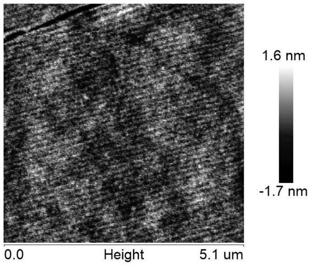
[0066] Adopt the preparation method of memristor in embodiment 1, but in SiO x In the preparation of the dielectric layer, room temperature ammonia catalytic curing method is adopted, which is as follows: the container with 10% ammonia water is placed in a closed environment to form an ammonia atmosphere, and the bottom electrode / Place the glass sheet in this airtight ammonia gas atmosphere and keep it at 25°C for 24h to obtain SiO x Dielectric layer, the resulting memristor structure is Ag / SiO x / Au / glass.
[0067] According to XRD analysis, it can be seen that the prepared SiO x The dielectric layer has a random structure; ellipsometer tests SiO x The thickness of the layer is 36.3nm; the oxygen-silicon ratio of silicon oxide x=1.45 is obtained by XPS characterization, and there is 6.25wt% nitrogen atom doping; AFM characterizes SiO x surface morphology from Figure 4 It can be seen in SiO x The surface is smooth and uniform, without cracks and voids, and the roughnes...
PUM
| Property | Measurement | Unit |
|---|---|---|
| thickness | aaaaa | aaaaa |
| thickness | aaaaa | aaaaa |
| diameter | aaaaa | aaaaa |
Abstract
Description
Claims
Application Information
 - R&D Engineer
- R&D Manager
- IP Professional
- Industry Leading Data Capabilities
- Powerful AI technology
- Patent DNA Extraction
Browse by: Latest US Patents, China's latest patents, Technical Efficacy Thesaurus, Application Domain, Technology Topic, Popular Technical Reports.
© 2024 PatSnap. All rights reserved.Legal|Privacy policy|Modern Slavery Act Transparency Statement|Sitemap|About US| Contact US: help@patsnap.com