
High-performance delta-CsPbI3 film memristor and preparation method thereof

A memristor and high-performance technology, applied in the field of high-performance δ-CsPbI3 thin film memristor and its preparation, can solve problems such as SET voltage reduction, and achieve the effects of simple preparation, low cost and simple method

Pending Publication Date: 2022-07-29
NORTH CHINA ELECTRIC POWER UNIV (BAODING)
View PDF0 Cites 0 Cited by
  • Summary
  • Abstract
  • Description
  • Claims
  • Application Information

AI Technical Summary

Problems solved by technology

In addition, compared with other memristor materials, the δ-CsPbI-based 3 There is still room for further reduction in the SET voltage of thin film memristors

Method used


Image

  • High-performance delta-CsPbI3 film memristor and preparation method thereof
  • High-performance delta-CsPbI3 film memristor and preparation method thereof
  • High-performance delta-CsPbI3 film memristor and preparation method thereof

Examples


Embodiment 1

[0039] A high-performance δ-CsPbI 3 The preparation method of thin film memristor comprises the following steps:

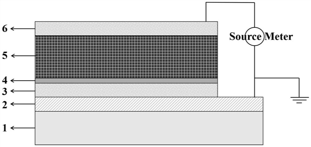
[0040] 1) Prepare clean FTO: First prepare the FTO conductive glass substrate composed of glass substrate 1 and FTO film 2, cut the FTO conductive glass into a size of 15mm × 13mm, and perform simple cleaning; then soak it in potassium dichromate In the solution for 20 minutes, clean the potassium dichromate, then wipe the surface with a non-woven fabric with detergent water; ultrasonically clean with deionized water and ethanol for 20 minutes; put the cleaned FTO into vacuum drying Dry in the oven; finally, sintering at 500℃ for 30 minutes in a flat furnace to remove organic impurities on the surface.

[0041] Evaporating the bottom electrode Ag film 3 on the surface of the FTO conductive glass: due to the appropriate roughness of the FTO, the bonding force of the Ag film can be significantly enhanced. At the same time, the use of the FTO is equivalent to leavin...


PUM

PropertyMeasurementUnit
thicknessaaaaaaaaaa
thicknessaaaaaaaaaa
thicknessaaaaaaaaaa

Abstract

The invention discloses a high-performance delta-CsPbI3 film memristor and a preparation method thereof, and belongs to the technical field of memristors. The structure of the delta-CsPbI3 thin film memristor sequentially comprises an FTO conductive glass substrate, a bottom electrode Ag film, an AgOx interface layer, a delta-CsPbI3 thin film and a top electrode Ag film from bottom to top. According to the delta-CsPbI3 thin film memristor, a yellow-phase delta-CsPbI3 thin film is deposited on the surface of a naturally oxidized amorphous AgOx layer, and an AgOx interface layer is beneficial for delta-CsPbI3 to form a continuous thin film and plays a key role in promoting formation of conductive Ag wires in the thin film. The memristor has nonvolatile bipolar resistance switching and storage characteristics, has an instantaneous setting / resetting phenomenon, a great switching ratio, low working voltage and extremely long data retention time, and greatly improves the application value of the CsPbI3 memristor.

Description

technical field [0001] The invention belongs to the technical field of memristors, in particular to a high-performance δ-CsPbI 3 Thin film memristor and method of making the same. Background technique [0002] As a typical non-volatile memory device, resistance-switching random access memory (RRAM) has excellent simple structure, scalability, fast switching speed, low power consumption and high integration, and is suitable for next-generation computing systems. The information storage and processing of NAND provides promising applications as a promising candidate memory to replace negative memory and (NAND) flash memory. RRAM is based on the resistance switching (RS) effect, which originates from the sudden resistance change of the device, is reversible bistable and non-volatile. The main evaluation parameters of memristor performance include operating voltage, current switching ratio, cycle life, retention time, erasing and writing time, etc. RRAM usually has a sandwich ...

Claims


Application Information

Patent Timeline
Patent Type & Authority Applications(China)
IPC IPC(8): H01L45/00
CPCH10N70/801H10N70/24H10N70/881H10N70/011
Inventor 许佳姚建曦姚程亮
Owner NORTH CHINA ELECTRIC POWER UNIV (BAODING)
Learn More