Manufacturing method of organic electroluminescent substrate
A manufacturing method and electroluminescence technology, which are applied to circuits, electrical components, electrical solid devices, etc., can solve the problems of inconsistent film layer morphology and thickness, affecting the display effect of display devices, etc., and achieve the effect of improving uniformity.
- Summary
- Abstract
- Description
- Claims
- Application Information
AI Technical Summary
Problems solved by technology
Method used
Image
Examples
Embodiment Construction
[0041] Specific embodiments of the present invention will be described in detail below in conjunction with the accompanying drawings. It should be understood that the specific embodiments described here are only used to illustrate and explain the present invention, and are not intended to limit the present invention.
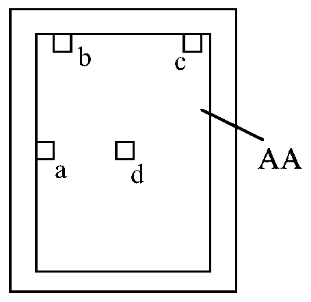
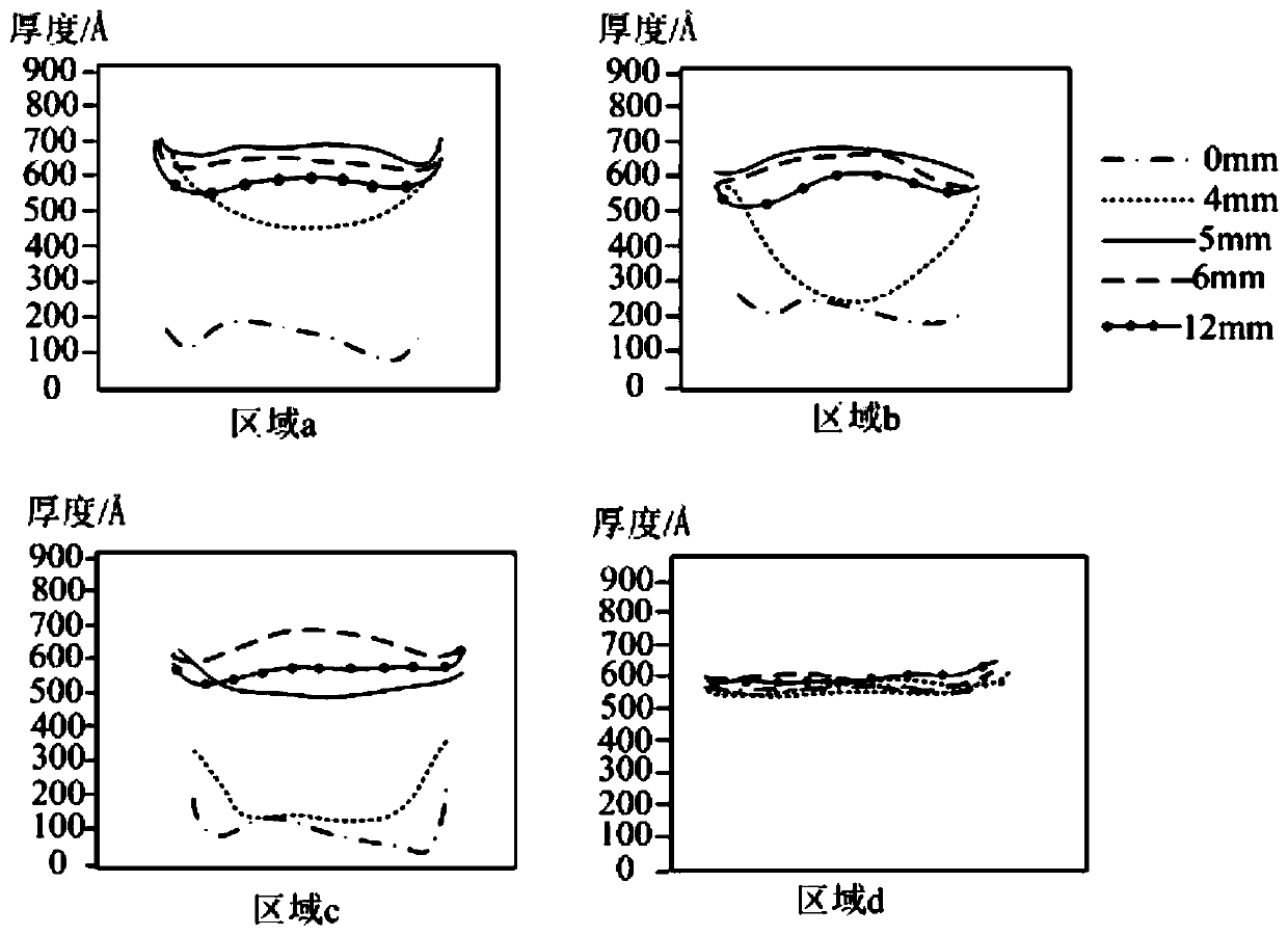
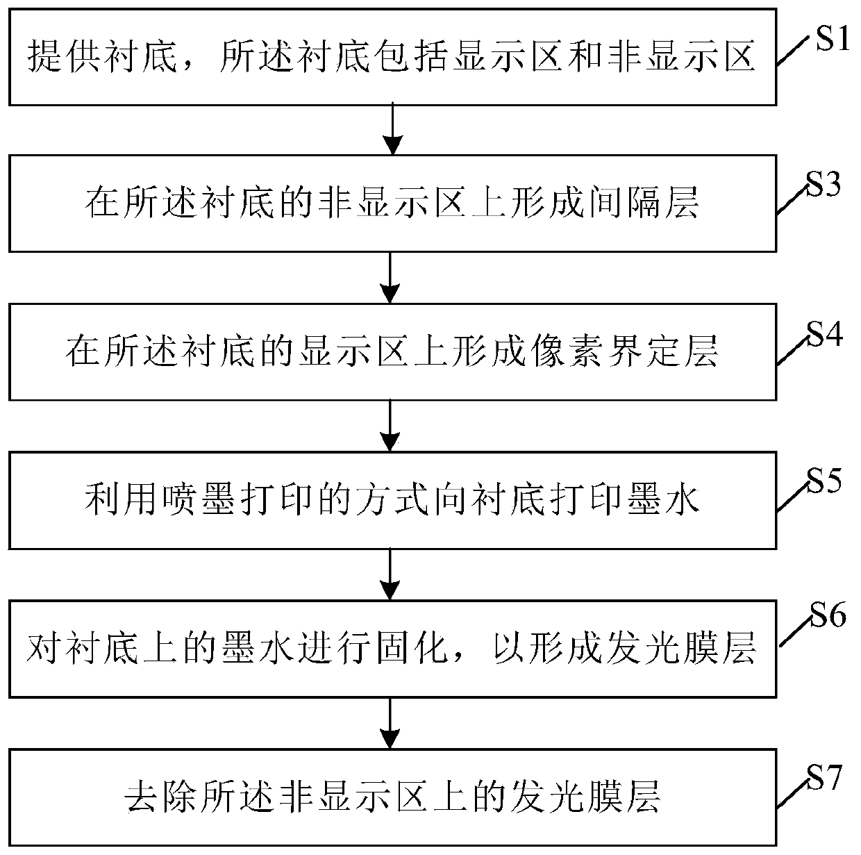
[0042] When inkjet printing is performed, the solvent atmosphere at the edge of the printing area is thinner, and the solvent atmosphere in the middle of the printing area is thicker. However, in the prior art, when inkjet printing is performed, the inkjet printing area does not exceed the display area, or exceeds the display area. This will lead to a large difference between the solvent atmosphere at the edge of the display area and the solvent atmosphere in the middle of the display area, resulting in the film layer formed in the pixels in the middle of the display area and the film layer formed in the pixels at the edge of the display area The thickness and p...
PUM
 Abstract
Description
Claims
Application Information


