

Shift register, array substrate and driving method thereof, and display device
A shift register and shift register technology are applied in the fields of shift registers, array substrates and driving methods thereof, and display devices, and can solve problems such as inability to output control signals by gate lines and increased power consumption of display panels.
- Summary
- Abstract
- Description
- Claims
- Application Information
AI Technical Summary
Problems solved by technology
Method used
Image


Examples
Embodiment 1
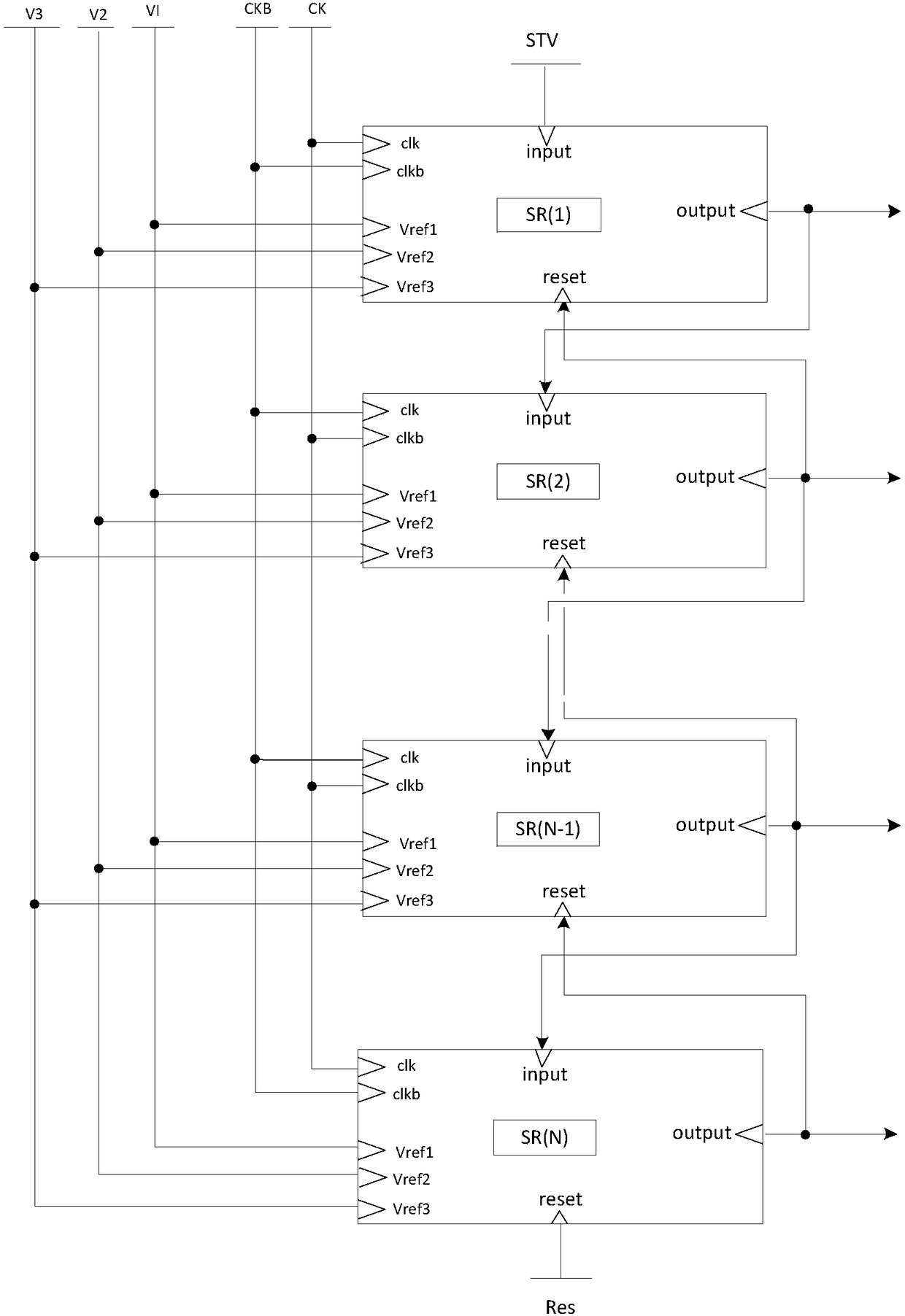
[0071] by image 3 shown as an example of a shift register, where image 3 The transistors in the shift register shown are all P-type transistors, the first reference voltage signal terminal VREF1 is at low potential, and the third reference signal terminal VREF3 is at high potential. The timing diagram of the corresponding shift register is as follows Figure 4 shown.
[0072] In the t1 stage, INPUT=0, CLK=0, CLKB=1, PW1=1, PW2=0.
[0073] The signal of the first clock signal terminal CLK turns on the seventh transistor M7, and the signal of the input signal terminal INPUT is respectively provided to the first pole of the ninth transistor M9 and the gate of the tenth transistor M10, because the first reference voltage signal terminal The voltage of VREF1 is low potential, the ninth transistor M9 is turned on, so that the potential of the first node N1 is low level, and the tenth transistor M10 is turned on to provide the signal of the first clock signal terminal CLK to the...
Embodiment 2
[0079] by image 3 shown as an example of a shift register, where image 3 The transistors in the shift register shown are all P-type transistors, the first reference signal terminal is low potential, the first reference voltage signal terminal and the second reference signal terminal are the same signal terminal, and the third reference signal terminal is high potential. The corresponding timing diagram of another above-mentioned shift register is as follows Figure 5 shown.
[0080] In the t1 stage, INPUT=0, CLK=0, CLKB=1, PW1=0, PW2=1.
[0081] The signal of the first clock signal terminal CLK turns on the seventh transistor M7, and the signal of the input signal terminal INPUT is respectively provided to the first pole of the ninth transistor M9 and the gate of the tenth transistor M10, because the first reference voltage signal terminal The voltage of VRFE1 is low potential, the ninth transistor M9 is turned on, so that the potential of the first node N1 is low level, ...
PUM
 Abstract
Description
Claims
Application Information