Supercharge Your Innovation With Domain-Expert AI Agents!

Process of forming semiconductor apparatus mounting on substrate

一种安装基板、半导体的技术,应用在半导体器件、半导体/固态器件制造、半导体/固态器件零部件等方向,能够解决半导体芯片与组装基板结合强度降低、小浸润性等问题

Active Publication Date: 2018-08-28
SUMITOMO ELECTRIC DEVICE INNOVATIONS
View PDF8 Cites 0 Cited by
  • Summary
  • Abstract
  • Description
  • Claims
  • Application Information

AI Technical Summary

Problems solved by technology

However, in the case where a semiconductor material (usually the semiconductor substrate of the semiconductor chip) is exposed on the backside of the semiconductor chip, this semiconductor material generally exhibits less wettability with respect to the solder material, which may make the semiconductor chip and the assembly substrate reduced bond strength

Method used


Image

  • Process of forming semiconductor apparatus mounting on substrate
  • Process of forming semiconductor apparatus mounting on substrate
  • Process of forming semiconductor apparatus mounting on substrate

Examples


Embodiment Construction

[0014] Next, embodiments of the present invention will be described with reference to the drawings. In the description of the embodiments, reference numerals or symbols identical to or similar to each other will refer to elements identical to or similar to each other, and explanations will not be repeated.

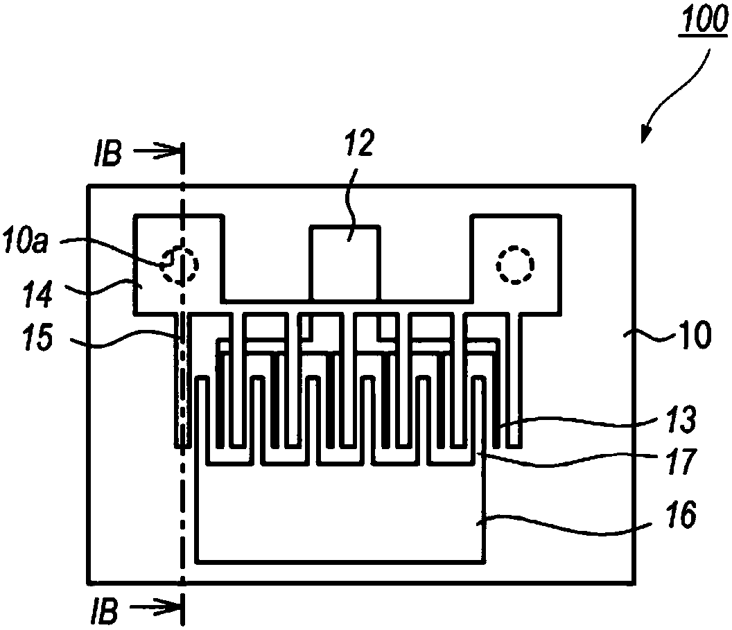
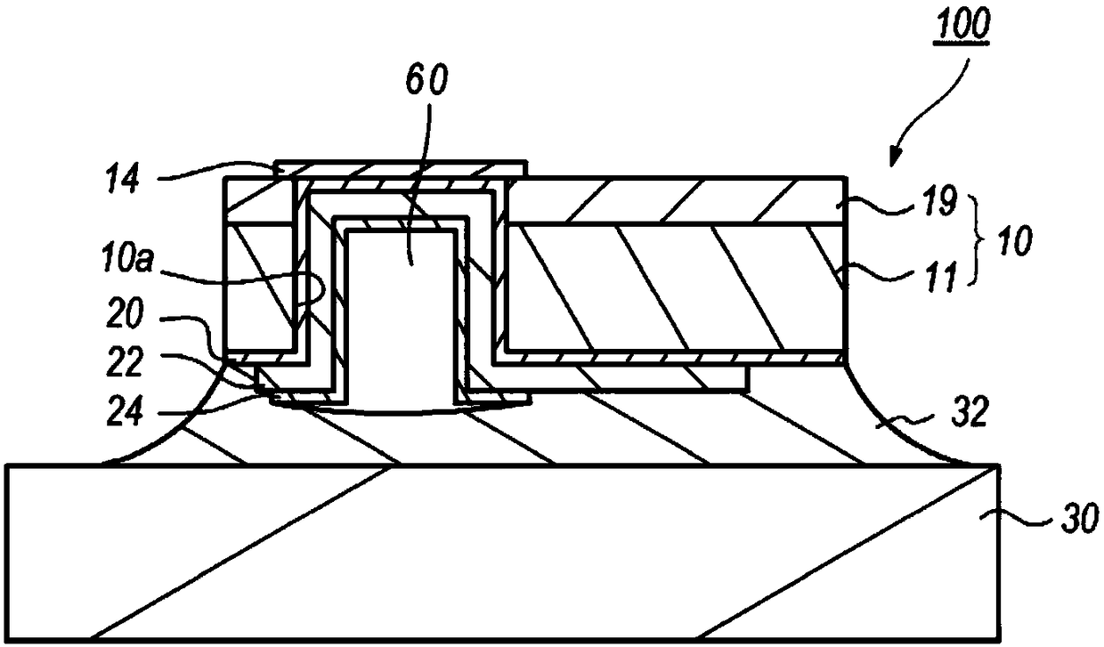
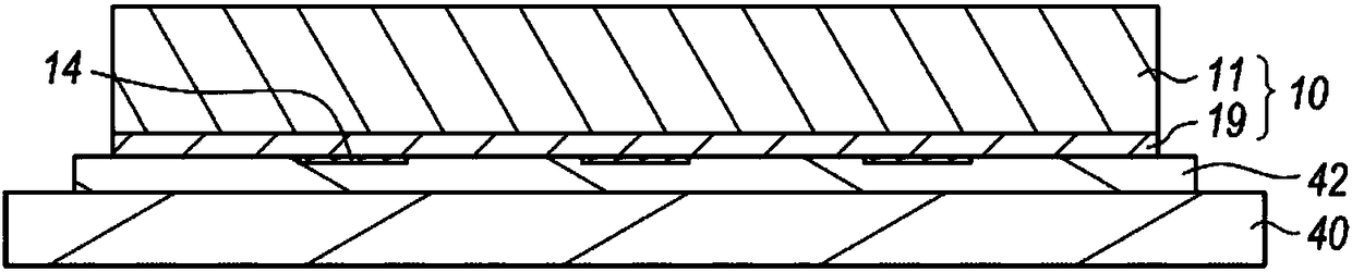
[0015] Figure 1A A plan view of a semiconductor device 100 according to a first embodiment of the present invention is shown. The semiconductor device 100 is a field effect transistor (FET) type, and the semiconductor device 100 includes a substrate 10, a gate pad 12, a gate finger (gatefinger) 13, a source pad 14, a source finger 15, a drain pad 16 and the drain finger 17. The epitaxial substrate 10 may include an insulating substrate 11 made of silicon carbide (SiC) and an epitaxial layer 19 grown on the insulating substrate 11 . The epitaxial layer 19 includes a channel layer made of gallium nitride (GaN) (the channel layer is sometimes called a carrier transport lay...


PUM


Abstract

A process of forming a semiconductor apparatus is disclosed. The process includes steps of: depositing a first metal layer containing Ni in a back surface of a substrate, plating the back surface of the substrate so as to expose the first metal layer in a portion of the scribe line, depositing a third metal layer on the whole back surface of the substrate, and selectively removing the third metallayer in the portion of the scribe line so as to leave the first metal layer in the scribe line.

Description

technical field [0001] The present invention relates to a method of forming a semiconductor device, and in particular, the present invention relates to a method capable of enhancing the bonding strength of a semiconductor device and an assembly substrate. Background technique [0002] The semiconductor chip is usually mounted on the assembly substrate using, for example, a solder material such as a eutectic alloy or solder having a low melting point, or a conductive resin or the like. Japanese Patent Application Publication No. JP-2015-035495A discloses a technique of mounting a semiconductor device on an assembly substrate. However, in the case where a semiconductor material (usually the semiconductor substrate of the semiconductor chip) is exposed on the backside of the semiconductor chip, this semiconductor material generally exhibits less wettability with respect to the solder material, which may make the semiconductor chip and the assembly substrate bond strength is re...

Claims


Application Information

Patent Timeline
Patent Type & Authority Applications(China)
IPC IPC(8): H01L21/60H01L23/488
CPCH01L24/29H01L24/83H01L2224/29155H01L2224/29171H01L2224/29166H01L2224/83801H01L21/76898H01L23/481H01L2224/13009H01L24/11H01L24/03H01L24/05H01L24/13H01L24/94H01L2224/32506H01L2224/83411H01L2224/83444H01L24/32
Inventor 江森正臣
Owner SUMITOMO ELECTRIC DEVICE INNOVATIONS
Features
  • R&D
  • Intellectual Property
  • Life Sciences
  • Materials
  • Tech Scout
  • Unparalleled Data Quality
  • Higher Quality Content
  • 60% Fewer Hallucinations
Learn More