Integrated chip processing device

A processing device and integrated chip technology, applied in the direction of transportation and packaging, conveyor objects, electrical components, etc., can solve problems such as unstable processing positions, improper coordination, rough processing procedures, etc., to facilitate maintenance and improve efficiency and effects, highly automated effects

Inactive Publication Date: 2018-09-04
NINGHAI LIHANG ELECTROMECHANICAL EQUIP DESIGN CO LTD
View PDF0 Cites 1 Cited by
  • Summary
  • Abstract
  • Description
  • Claims
  • Application Information

AI Technical Summary

Problems solved by technology

[0002] At present, integrated chips have become the essential core electronic components of global electronic products. There are also certain strict requirements for the processing of integrated chips. General and traditional integrated chip packaging equipment adopt rough processing procedures and complicated operations, which will cause irreversible effects. , the inappropriate coordination between the various processes affects the performance of the chip. At the same time, due to the unstable processing position, the effect of each process is not good, and the circuits of each layer are broken or short-circuited. Therefore, an integrated chip processing device is urgently needed at present.

Method used


Image

  • Integrated chip processing device
  • Integrated chip processing device
  • Integrated chip processing device

Examples


Embodiment Construction

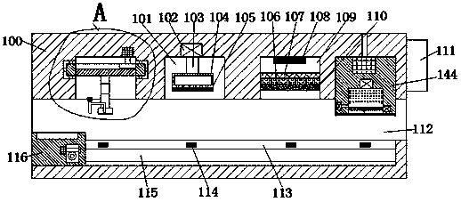
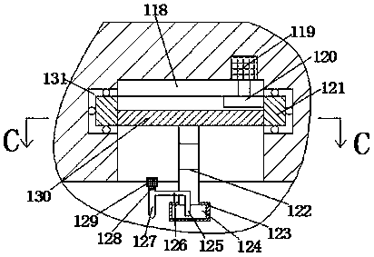
[0022] Such as Figure 1-Figure 7As shown, an integrated chip processing device of the present invention includes a processing machine body 100 and a conveying cavity 112 arranged in the processing machine body 100 through the left and right sides. The metal sputtering chamber 118, the coating photoresist chamber 101, the photolithography chamber 109 and the first guide chute communicated with the conveying chamber 112, the processing machine body 100 is provided with an opening upwards and communicated with the conveying chamber 112 The second guide groove 113, the front and rear inner walls of the second guide groove 113 are connected with a guide rail groove 115 that is symmetrical and extends along the second guide groove 113, and the rear end of the second guide groove 113 The inner wall is provided with a first displacement sensor 114 directly below the center line of the metal sputtering chamber 118, the coating photoresist chamber 101, the photolithography chamber 109 ...


PUM


Abstract

The invention discloses an integrated chip processing device, and the device comprises a processing unit body, and a conveying cavity which is disposed in the processing unit body and is laterally through. The interior of the processing unit body is sequentially provided with a metal spluttering coating cavity, a coating light resistance cavity, a photoetching cavity and a first sliding guide groove from the left to the right, wherein the openings of the metal spluttering coating cavity, the coating light resistance cavity, the photoetching cavity and the first sliding guide groove face downwards and are communicated with the conveying cavity. The interior of the processing unit body is provided with a second sliding guide groove which is communicated with the conveying cavity, wherein theopening of the second sliding guide groove face upwards. The front and rear inner walls of the second sliding guide groove are symmetrically provided with guide rail grooves in a communicated manner,wherein the guide rail grooves extend along the second sliding guide groove. The rear end inner wall of the second sliding guide groove is provided with a first displacement sensor which is located exactly below the central axis of the metal spluttering coating cavity, the coating light resistance cavity, the photoetching cavity and the first sliding guide groove. The device is simple in structure, is convenient to operate, is precise in processing, and improves the processing efficiency and effect of an integrated chip.

Description

technical field [0001] The invention relates to the technical field of integrated chip processing, in particular to an integrated chip processing device. Background technique [0002] At present, integrated chips have become the essential core electronic components of global electronic products. There are also certain strict requirements for the processing of integrated chips. General and traditional integrated chip packaging equipment adopt rough processing procedures and complicated operations, which will cause irreversible effects. , Improper coordination between the various processes affects chip performance. At the same time, due to the unstable processing position, the effects of each process are not good, and the circuits of each layer are broken or short-circuited. Therefore, an integrated chip processing device is urgently needed at present. Contents of the invention [0003] The technical problem to be solved by the present invention is to provide an integrated c...

Claims


Application Information

Patent Timeline
Patent Type & Authority Applications(China)
IPC IPC(8): H01L21/67H01L21/677
CPCH01L21/67706H01L21/67184
Inventor 张叶莎
Owner NINGHAI LIHANG ELECTROMECHANICAL EQUIP DESIGN CO LTD
Why Eureka
Try Eureka