Tin-isolated flexible circuit board PAD and manufacturing method thereof
A technology for flexible circuit boards and manufacturing methods, which is applied to printed circuits, printed circuits, printed circuit components, etc., can solve the problems of lower yield, yield loss, and insufficient tin content, etc., to increase yield and reduce yield loss effect
- Summary
- Abstract
- Description
- Claims
- Application Information
AI Technical Summary
Problems solved by technology
Method used
Image
Examples
Embodiment 1
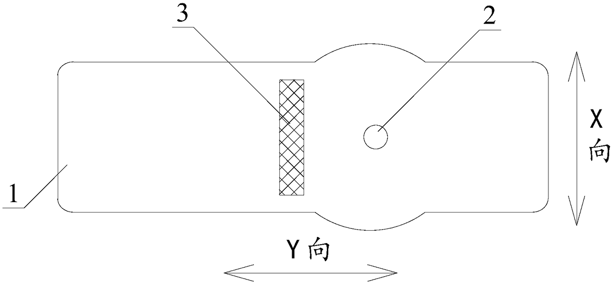
[0026] Such as figure 1 Shown is an embodiment 1 of a tin-separated flexible circuit board PAD according to the present invention. The flexible circuit board PAD1 is provided with a through hole 2, and one side of the flexible circuit board PAD 1 is also provided with a tin-separated slot 3. The X-direction dimension of the tin bath 3 is 70% of the X-direction dimension of the flexible circuit board PAD 1, the Y-direction dimension of the tin bath 3 is 6% of the Y-direction dimension of the flexible circuit board PAD 1, and the depth of the tin bath 3 is 4 μm, the distance between the tin slot 3 and the through hole 2 is 9% of the Y-direction dimension of the flexible circuit board PAD 1 , and the cross section of the tin slot 3 is rectangular.
[0027] The manufacturing method of this embodiment is as follows: the surface of the flexible circuit board PAD1 is plated with gold and nickel to form a gold-plated nickel layer, and the spacers are sequentially etched on the gold-pl...
Embodiment 2
[0029] The difference from Example 1 is that the X-direction dimension of the tin slot 3 is 50% of the X-direction dimension of the flexible circuit board PAD 1, and the Y-direction dimension of the tin slot 3 is 4 of the Y-direction dimension of the flexible circuit board PAD 1. %, the depth of the tin slot 3 is 5 μm, the distance between the tin slot 3 and the through hole 2 is 10% of the Y-direction dimension of the flexible circuit board PAD 1, and the cross section of the tin slot 3 is circular.
[0030] The manufacturing method of this embodiment is as follows: the surface of the flexible circuit board PAD 1 is plated with copper to form a copper plating layer, and a tin separation groove is etched on the copper plating layer and the surface of the flexible circuit board PAD 1 with a laser according to the preset size and distance 3. Protect the tin tank 3, and then carry out chemical immersion gold to form an immersion gold layer.
Embodiment 3
[0032] The difference from Example 1 is that the X-direction dimension of the tin slot 3 is 60% of the X-direction dimension of the flexible circuit board PAD 1, and the Y-direction dimension of the tin slot 3 is 8 of the Y-direction dimension of the flexible circuit board PAD 1 %, the depth of the tin slot 3 is 2.5 μm, the distance between the tin slot 3 and the through hole 2 is 8.5% of the Y-direction dimension of the flexible circuit board PAD1, and the cross section of the tin slot 3 is elliptical.
PUM
 Abstract
Description
Claims
Application Information
 - R&D
- Intellectual Property
- Life Sciences
- Materials
- Tech Scout
- Unparalleled Data Quality
- Higher Quality Content
- 60% Fewer Hallucinations
Browse by: Latest US Patents, China's latest patents, Technical Efficacy Thesaurus, Application Domain, Technology Topic, Popular Technical Reports.
© 2025 PatSnap. All rights reserved.Legal|Privacy policy|Modern Slavery Act Transparency Statement|Sitemap|About US| Contact US: help@patsnap.com

