OLED product and production method thereof

A production method and product technology, applied in the production of OLED products, in the field of OLED products, can solve problems such as poor compatibility, and achieve the effects of improving product quality and production efficiency, smooth surface, and improved sensitivity

Active Publication Date: 2018-09-14
TRULY SEMICON
View PDF15 Cites 0 Cited by
  • Summary
  • Abstract
  • Description
  • Claims
  • Application Information

AI Technical Summary

Problems solved by technology

[0003] The technical problem to be solved by the present invention is to be able to solve the problem of poor compatibility between the technical scheme of adding auxiliary metal and the Mo alloy protection scheme in the production process of the existing OLED products using ON CELL technology, and to effectively improve product quality and production efficiency

Method used


Image

  • OLED product and production method thereof
  • OLED product and production method thereof

Examples


Embodiment 1

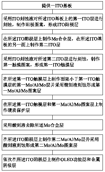
[0028] Such as figure 1 As shown, it represents a manufacturing method of an OLED product provided by the present invention. The manufacturing method of the OLED product specifically includes the following steps:

[0029] Step 1, providing an ITO substrate; specifically, the step 1 may include: step 1.1, providing a transparent substrate; step 1.2, making a SiO2 layer on the transparent substrate; step 1.2, plating the second SiO2 layer on the SiO2 layer One ITO layer. Wherein, the transparent substrate is preferably a glass substrate, and its surface is polished before making the SiO2 layer, and the thickness of the SiO2 layer is 200 to 300 Å; the manufacturing method of the first ITO layer is magnetron sputtering, The deposition temperature is between 200-280°C, and the thickness can be 800-2200Å. After the first ITO layer is manufactured, the surface needs to be soft-polished to control its surface roughness Ra<10Å.

[0030] Step 2, using ITO etchant to etch the first IT...

Embodiment 2

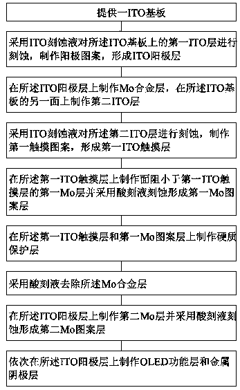
[0041] The principle of this embodiment is the same as that of the previous embodiment, and the structure is similar. The only difference is that, as figure 2 As shown, the first Mo / Al / Mo layer is replaced by the first Mo layer, and the first Mo / Al / Mo pattern layer is replaced by the first Mo pattern layer;

[0042] Specifically, a method for manufacturing an OLED product provided in this embodiment specifically includes the following steps:

[0043] Step 1, providing an ITO substrate;

[0044] Step 2, using an ITO etchant to etch the first ITO layer on the ITO substrate to make an anode pattern to form an ITO anode layer;

[0045] Step 3, making a Mo alloy layer on the ITO anode layer, and making a second ITO layer on the other side of the ITO substrate;

[0046] Step 4, using ITO etchant to etch the second ITO layer to make a first touch pattern to form a first ITO touch layer;

[0047] Step 5. On the first ITO touch layer, make a first Mo layer with an area resistance l...

Embodiment 3

[0054] This embodiment provides an OLED product, which is obtained by using the method for manufacturing an OLED product described in any of the above embodiments.


PUM

PropertyMeasurementUnit
thicknessaaaaaaaaaa
thicknessaaaaaaaaaa
thicknessaaaaaaaaaa

Abstract

The invention provides an OLED product and a production method thereof. The production method comprises the following steps: 1, providing an ITO substrate; 2, etching a first ITO layer on the ITO substrate to form an ITO anode layer; 3, producing an Mo alloy layer on the ITO anode layer, and producing a second ITO layer on the other surface of the ITO substrate; 4, etching the second ITO layer toform a first ITO touch layer; 5, producing and etching a first Mo/Al/Mo pattern layer on the first ITO touch layer; 6, producing a hard protective layer on the first ITO touch layer and the first Mo/Al/Mo pattern layer; 7, removing the Mo alloy layer; 8, producing and etching a second Mo/Al/Mo pattern layer on the ITO anode layer; 9: producing an OLED functional layer and a metal cathode layer. Bythe production method, the problem of poor compatibility between the existing technical scheme of adding auxiliary metal in the process of producing an OLED product by an ON CELL technology and an Moalloy protection scheme can be solved, and the product quality and the production efficiency can be effectively improved.

Description

technical field [0001] The invention relates to the field of display technology, in particular to a method for manufacturing an OLED product and the OLED product. Background technique [0002] ON CELL technology is one of the best solutions for integrated touch function of OLED products. This technology sets the ITO touch layer on the light-emitting surface of OLED products. When etching the touch pattern of the ITO touch layer, it is necessary to first place the touch pattern on the back of the substrate. The ITO anode layer is protected, and the commonly used protection method is to silk screen or paste a protective film on the ITO anode layer. Although this type of protection method is relatively simple in equipment and process, it is prone to problems such as residual glue and ITO anode layer being crushed, and the protective film needs to be manually torn off after the ITO touch layer is etched, which is not conducive to the automation and high efficiency of the process...

Claims


Application Information

Patent Timeline
Patent Type & Authority Applications(China)
IPC IPC(8): H01L51/56
CPCH10K71/00
Inventor 罗志猛赵云
Owner TRULY SEMICON
Why Eureka
Try Eureka