
Method of drilling hole in PCB

A drill-through and drill technology, which is applied in the field of PCB manufacturing, can solve the problems of inability to adjust flexibly and completely solve the problems such as the pull-off and reliability of the inner layer thick copper drilling pad, so as to reduce the damage of the drill and the hole wall. The effect of good quality and improved reliability

Active Publication Date: 2018-09-14
DONGGUAN SHENGYI ELECTRONICS +1
View PDF4 Cites 7 Cited by
  • Summary
  • Abstract
  • Description
  • Claims
  • Application Information

AI Technical Summary

Problems solved by technology

[0003] In the existing technology, the step-by-step drilling is carried out at a fixed ratio, that is, each time a fixed depth is drilled, it cannot be adjusted flexibly according to the actual situation, and it cannot completely solve the problems of pad pull-off and reliability caused by inner layer thick copper drilling

Method used


Image

  • Method of drilling hole in PCB
  • Method of drilling hole in PCB
  • Method of drilling hole in PCB

Examples


Embodiment 1

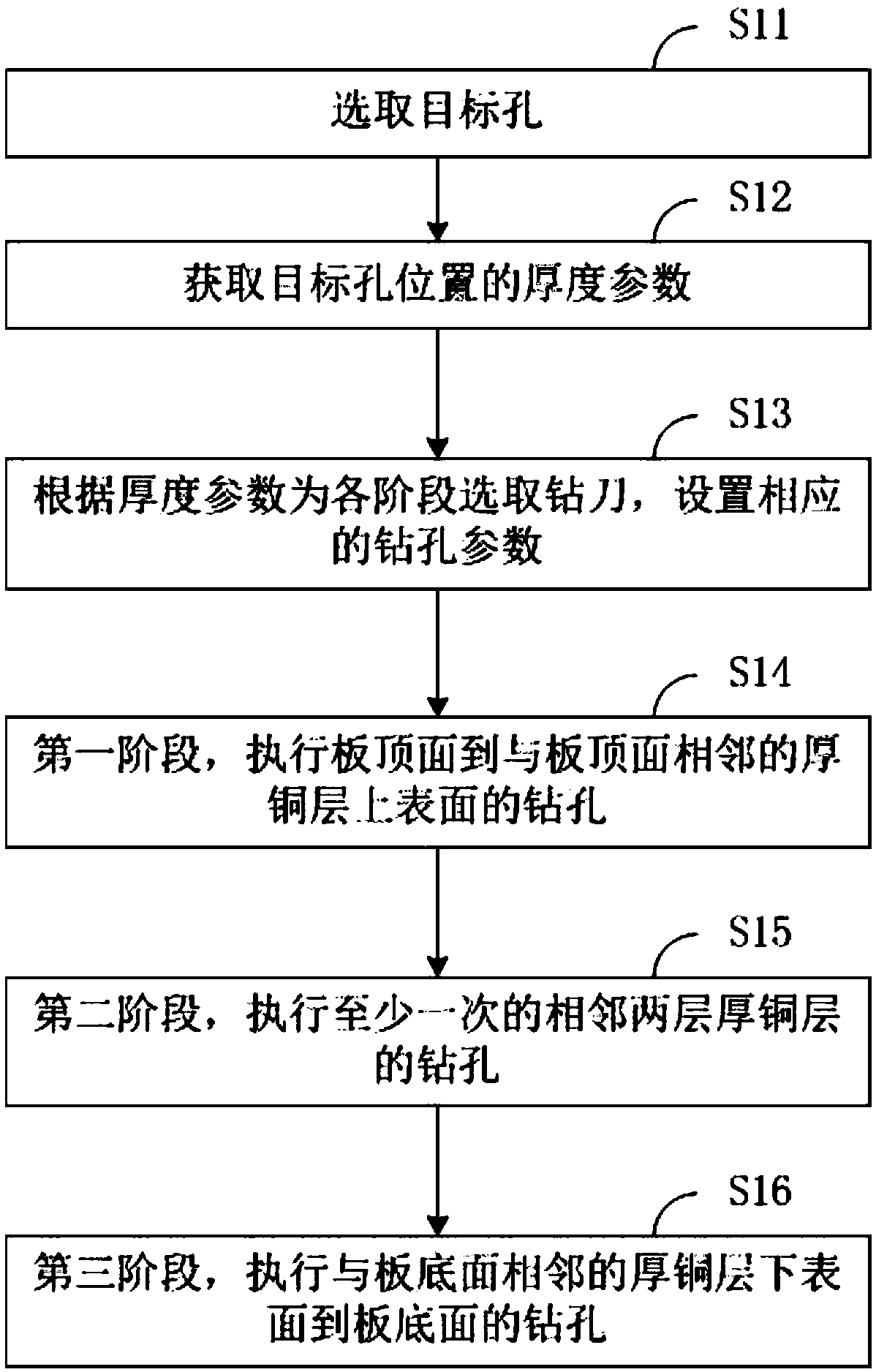
[0048] This embodiment provides a method for drilling holes on a PCB, which is suitable for manufacturing a PCB with a thick copper layer at the drilling position.

[0049] figure 1 It is a flowchart of a method for drilling holes on a PCB provided in this embodiment. Such as figure 1 As shown, the method includes the following steps:

[0050] S11, select the target hole.

[0051] The copper layer at the drilling position of the target hole includes a thick copper layer; the thick copper layer is a copper layer with a copper thickness ≥ 2OZ.

[0052] S12: Obtain the thickness parameter of the target hole position.

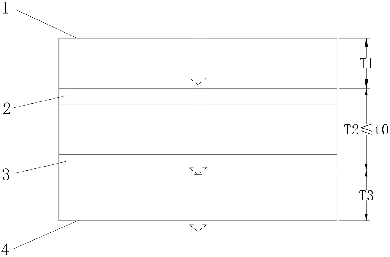
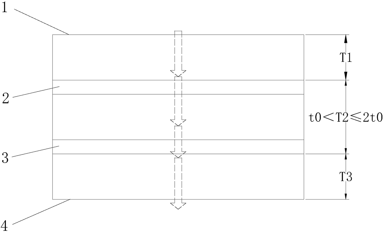
[0053] The drilling is divided into three stages. In the first stage, drilling is performed from the top surface of the board to the upper surface of the thick copper layer adjacent to the top surface of the board; in the second stage, the drilling of two adjacent thick copper layers is performed at least once. Drilling; In the third stage, drilling is performed from the l...

Embodiment 2

[0072] On the basis of the foregoing embodiment, this embodiment modifies the specific implementation method of step S15, and provides other drilling steps for the case of T2>2t0.

[0073] Figure 5 It is a schematic diagram of the drilling step of T2>2t0 in this embodiment. Take the PCB with 2 thick copper layers as an example, such as Figure 5 As shown, if T2>2t0, the number of cutting times is three times, which specifically includes the following steps:

[0074] Drill through the thick copper layer 2, and the drilling distance ≤ t0;

[0075] Drill to the upper surface of the lower thick copper layer 3;

[0076] Drill through the lower thick copper layer 3, the drilling distance ≤ t0.

[0077] Among them, t0 is the single maximum drilling distance through the thick copper layer, and t0≤1.5mm.

[0078] If the PCB includes multiple thick copper layers, the two adjacent thick copper layers form a group. For each group of T2, if T2>2t0, repeat the above steps. The thick copper layer t...


PUM


Abstract

The invention discloses a method of drilling a hole in a PCB, and relates to a production technology of the PCB. The method comprises the following steps of acquiring the thickness parameter at the position of a target hole and completing drilling in each stage according to the thickness parameter, and comprises the following specific steps: in a first stage, drilling from the top surface of the board to the upper surface of a thick copper layer adjacent to the top surface of the board; in a second stage, drilling two adjacent thick copper layers at least once; in a third stage, drilling fromthe lower surface of a thick copper layer adjacent to the bottom surface of the board to the bottom surface of the board, wherein the thick copper layer is a copper layer with the copper thickness being greater than or equal to 2OZ. By the method, according to the condition of the copper layers at the drilled position, the drilling stages are divided by using the thick copper layers as boundary points so as to complete drilling of a through hole step by step, so that selection of drilling tools and setting of drilling parameters according to the thicknesses of the copper layers in different drilling stages are facilitated so as to reduce wear on the drilling tools, and the through hole having good hole wall quality can be obtained and the reliability of a product is improved.

Description

Technical field [0001] The present invention relates to PCB manufacturing technology, in particular to a method for drilling holes on PCB. Background technique [0002] In the process of PCB drilling, the thickness of the board, the material filler, and the inner layer of copper will greatly wear the drill. If the drilling parameters are unreasonable, especially when the thickness of the plate is large (≥2mm), when the inner layer of copper is more thick, it is very easy to cause poor drilling hole walls, small holes due to burrs in the holes, and reflow soldering Quality issues such as post-layering. In order to improve this kind of problem, in the early stage, the method of step drilling is mainly used for production. [0003] In the prior art, the step-by-step drilling is carried out at a fixed ratio, that is, a fixed depth is drilled each time, which cannot be adjusted flexibly according to the actual situation, and cannot completely solve the problems of pad pull-off and rel...

Claims


Application Information

Patent Timeline
Patent Type & Authority Applications(China)
IPC IPC(8): H05K3/04H05K3/00
CPCH05K3/0047H05K3/04H05K2203/03H05K2203/1476
Inventor 万里鹏刘梦茹王祥纪成光王善进
Owner DONGGUAN SHENGYI ELECTRONICS
Learn More