Supercharge Your Innovation With Domain-Expert AI Agents!

High-speed reference voltage buffer with cross coupling filter network

A reference voltage buffering and filtering network technology, applied in instruments, adjusting electrical variables, control/regulating systems, etc., can solve the problems of large circuit area, capacitor consumption, large chip area, etc., to save chip area, improve response speed, Improve the effect of filtering

Active Publication Date: 2018-09-21
UNIV OF ELECTRONICS SCI & TECH OF CHINA
View PDF8 Cites 0 Cited by
  • Summary
  • Abstract
  • Description
  • Claims
  • Application Information

AI Technical Summary

Problems solved by technology

[0020] Aiming at the problems of large circuit area and slow response speed in the above-mentioned traditional reference voltage buffer structure, the present invention proposes a reference voltage buffer with a cross-coupling filter network. Under the premise of ensuring the filtering effect, the area of ​​the capacitor can be reduced It is close to 4 times, which solves the problem that the traditional CRC filter network consumes a large chip area for the capacitance to ground; in addition, based on changing the fixed resistor connected to the output terminal of the negative reference voltage Vrefb to a variable resistor, the negative reference voltage Vrefb and the overall The response speed reduces the power consumption of the circuit

Method used


Image

  • High-speed reference voltage buffer with cross coupling filter network
  • High-speed reference voltage buffer with cross coupling filter network
  • High-speed reference voltage buffer with cross coupling filter network

Examples


Embodiment Construction

[0042] The present invention will be further described below in conjunction with the accompanying drawings and embodiments.

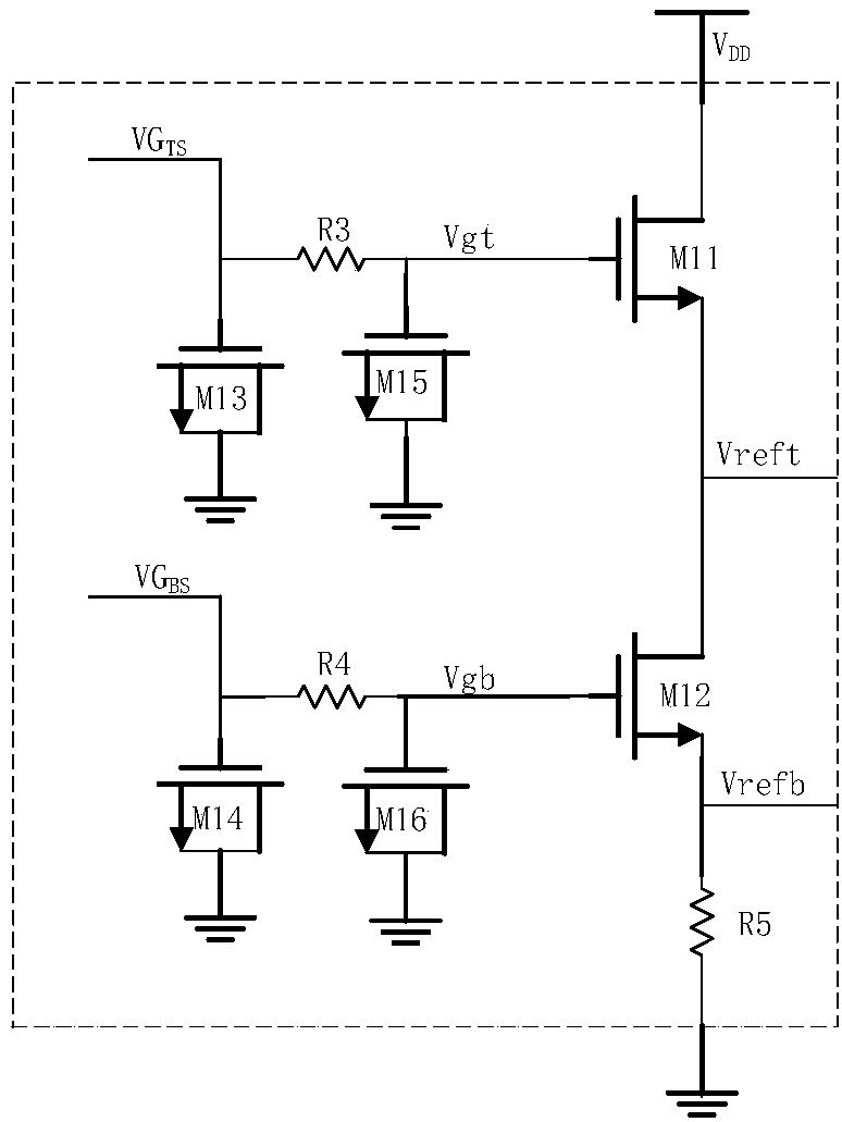
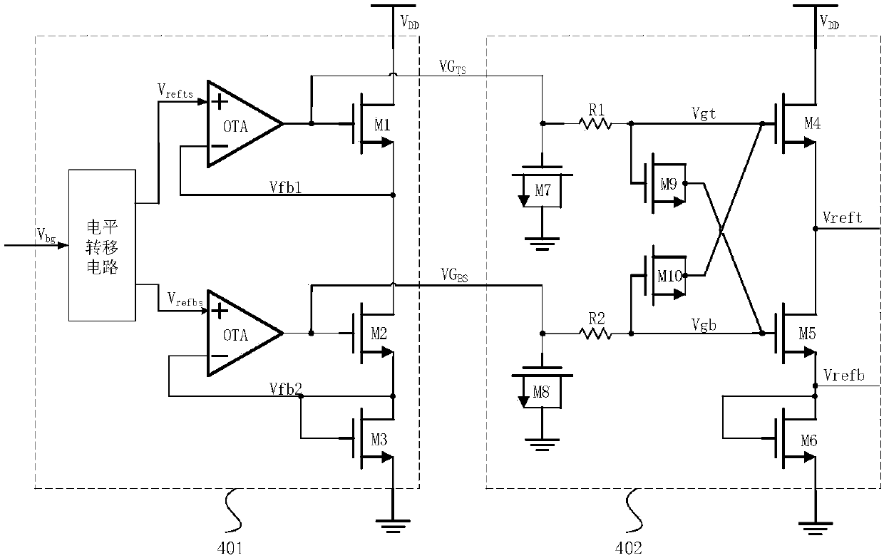
[0043] The reference voltage buffer proposed by the present invention is as image 3As shown, it includes the reference voltage generation module 401 of the previous stage and the reference voltage output buffer module 402 of the subsequent stage, wherein the reference voltage generation module 401 includes a level shift circuit, a first error amplifier, a second error amplifier, a first NMOS transistor M1 , the second NMOS transistor M2 and the third NMOS transistor M3, the respective substrates and sources of the first NMOS transistor M1, the second NMOS transistor M2 and the third NMOS transistor M3 are connected, and the input end of the level shift circuit is connected to the reference voltage Vbg , used to generate the primary positive reference voltage Vrefts and the primary negative reference voltage Vrefbs; the positive input terminal of the fi...


PUM


Abstract

The invention discloses a high-speed reference voltage buffer with a cross coupling filter network, and belongs to the technical field of analogue integrated circuits. The high-speed reference voltagebuffer with the cross coupling filter network comprises a reference voltage generating module and a reference voltage output buffering module. The reference voltage generating module comprises a level transfer circuit, two feedback circuits of which each is formed by an error amplifier and a source follower MOS tube and one diode-connected MOS tube. The reference voltage output buffering module comprises a CRC filter network, two source follower output stages and one diode-connected MOS tube. An externally given reference voltage produces a primary positive reference voltage and a primary negative reference voltage through the level transfer circuit, and after passing through the two feedback circuits, the voltages are input to the CRC filter network in the reference voltage output buffering module for filtering and processing from the output ends of two error amplifiers, and finally a positive reference voltage and a negative reference voltage are output through the output stages ofthe two source followers. The high-speed reference voltage buffer with the cross coupling filter network is capable of saving a chip area, and improving a response speed.

Description

technical field [0001] The invention belongs to the technical field of analog integrated circuits, in particular to a reference voltage buffer circuit with a cross-coupling filter network and fast response capability. Background technique [0002] The advancement of integrated circuit technology has continuously increased the working speed of digital circuits, requiring higher speeds for analog-to-digital converters ADC. However, with the improvement of ADC speeds, the requirements for the response speed of reference voltage buffers are also getting higher and higher, especially For a high-speed time-interleaved ADC, not only the reference voltage buffer is required to have a fast response speed, but also more stringent requirements are imposed on the mutual interference of the reference voltages between channels. In view of the above reasons, the high-speed reference voltage buffer circuit with a filter network with excellent filtering effect has become a research hotspot i...

Claims


Application Information

Patent Timeline
IPC IPC(8): G05F1/56
CPCG05F1/56
Inventor 李靖陈炳华罗建徐成阳宁宁吴克军
Owner UNIV OF ELECTRONICS SCI & TECH OF CHINA
Features
  • R&D
  • Intellectual Property
  • Life Sciences
  • Materials
  • Tech Scout
  • Unparalleled Data Quality
  • Higher Quality Content
  • 60% Fewer Hallucinations
Learn More