
Stable-contact solderless stamping terminal

A technology of stable contact and terminals, applied in the direction of connection, fixed connection, circuit, etc.

Inactive Publication Date: 2018-09-21
阜阳冈奇精密科技有限公司
View PDF3 Cites 0 Cited by
  • Summary
  • Abstract
  • Description
  • Claims
  • Application Information

AI Technical Summary

Problems solved by technology

[0004] Aiming at the deficiencies of the prior art, the present invention provides a solder-free stamping terminal with stable contact. By inventing the stamping terminal leg, the stamping terminal is punched out and closely matched with the PCB after assembly to ensure its holding force and electrical requirements. , eliminating cost waste and quality problems caused by manual soldering and wave soldering

Method used


Image

  • Stable-contact solderless stamping terminal

Examples


Embodiment Construction

[0016] The following will clearly and completely describe the technical solutions in the embodiments of the present invention with reference to the accompanying drawings in the embodiments of the present invention. Obviously, the described embodiments are only some, not all, embodiments of the present invention. Based on the embodiments of the present invention, all other embodiments obtained by persons of ordinary skill in the art without making creative efforts belong to the protection scope of the present invention.

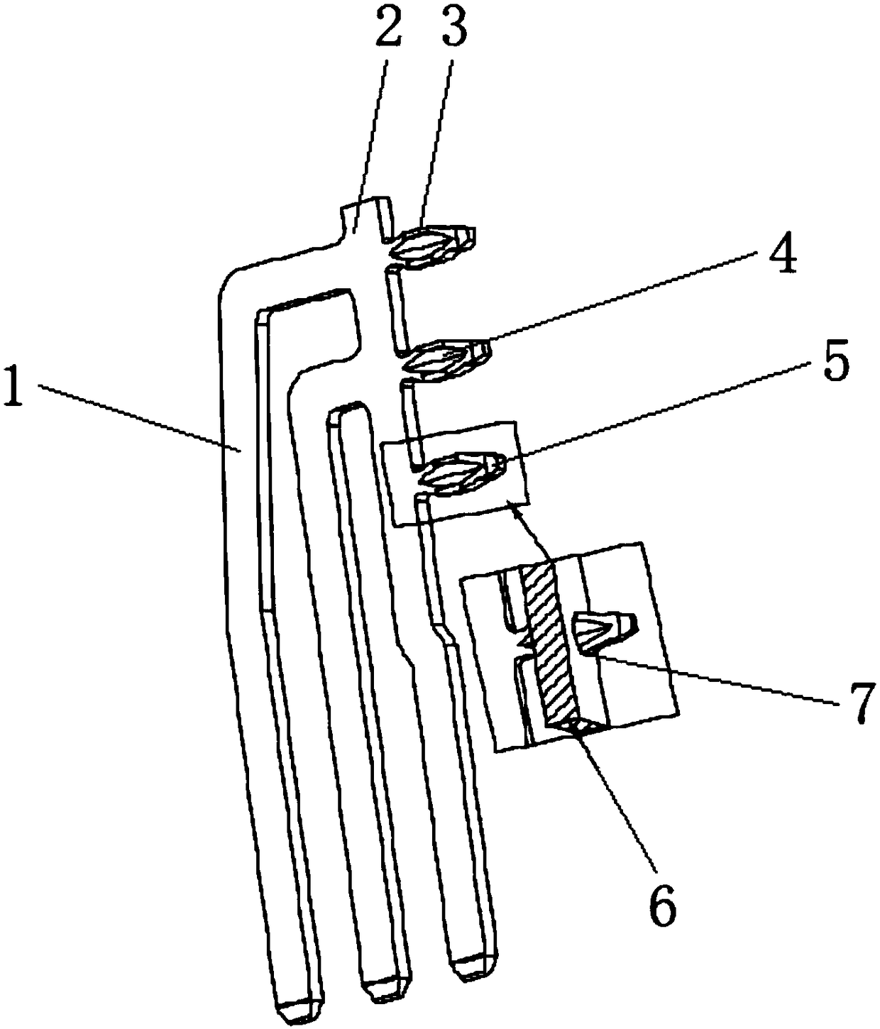
[0017] see figure 1 , a solderless stamping terminal with stable contact, including a terminal 1 and a PCB board 6, a leg 2 is welded on the terminal 1, and the opposite sides of the leg 2 are circular arc surfaces, so that it can reach the PCB hole to the maximum extent after being inserted into the PCB board 6 7. There are soldering points in 7, and there is a positioning point on both sides of the leg 2. Terminal 1 is inserted into the PCB hole 7 according ...


PUM


Abstract

The invention relates to the technical field of stamping terminal leg forming, and discloses a stable-contact solderless stamping terminal. The stable-contact solderless stamping terminal comprises aterminal and a PCB, wherein the terminal is soldered with a leg, and a leg R angle surface is designed on the surface of the leg.; two sides of the leg R angle surface are each welded with a leg embedded die, and the other two sides of the leg R angle surface are each provided with upper and lower grooves of the center of the leg; and the surface of the PCB is provided with a PCB hole. For the stable-contact solderless stamping terminal, by setting the upper and lower grooves of the center of the leg, during the process that the terminal is inserted into the PCB hole, the terminal is shrunk sothat the terminal can be inserted smoothly; and when the terminal is inserted into the PCB hole and is located, the terminal is expanded, thus enabling the R angle surface of the terminal to be moreclosely attached to the inside of the PCB hole, thus further guaranteeing the electrical performance.

Description

technical field [0001] The invention relates to the technical field of stamping terminal leg forming, in particular to a welding-free stamping terminal with stable contact. Background technique [0002] Solder-free stamping terminal is an accessory product suitable for electrical connection. It is industrially classified into the category of connectors and can be widely used in PCB assembly in industrial, consumer electronics and other electronic industries. In the current technology industry, soldering of stamped terminals (DIP plug-in components) is tin soldering, which is manifested in manual soldering, wave soldering and other methods. The disadvantages of the existing technology are high production cost and unstable product quality. The common quality problems are manifested in common welding problems such as empty soldering, virtual soldering, false soldering, and tin beads. In particular, the problem of false soldering cannot be found during the production inspection...

Claims


Application Information

Patent Timeline
Patent Type & Authority Applications(China)
IPC IPC(8): H01R12/58
CPCH01R12/58
Inventor 周玉振
Owner 阜阳冈奇精密科技有限公司
Features
  • Generate Ideas
  • Intellectual Property
  • Life Sciences
  • Materials
  • Tech Scout
  • Unparalleled Data Quality
  • Higher Quality Content
  • 60% Fewer Hallucinations
Learn More