Semiconductor component fuse structure and manufacturing method thereof
A technology of fuse structure and manufacturing method, which is applied in semiconductor/solid-state device manufacturing, semiconductor devices, semiconductor/solid-state device components, etc., can solve problems such as uniformity that cannot meet requirements, semiconductor component failure, circuit repair failure, etc., to achieve Meet high uniformity requirements, improve uniformity, and achieve good uniformity
- Summary
- Abstract
- Description
- Claims
- Application Information
AI Technical Summary
Problems solved by technology
Method used
Image

Examples
no. 1 example
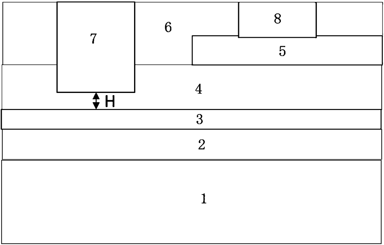
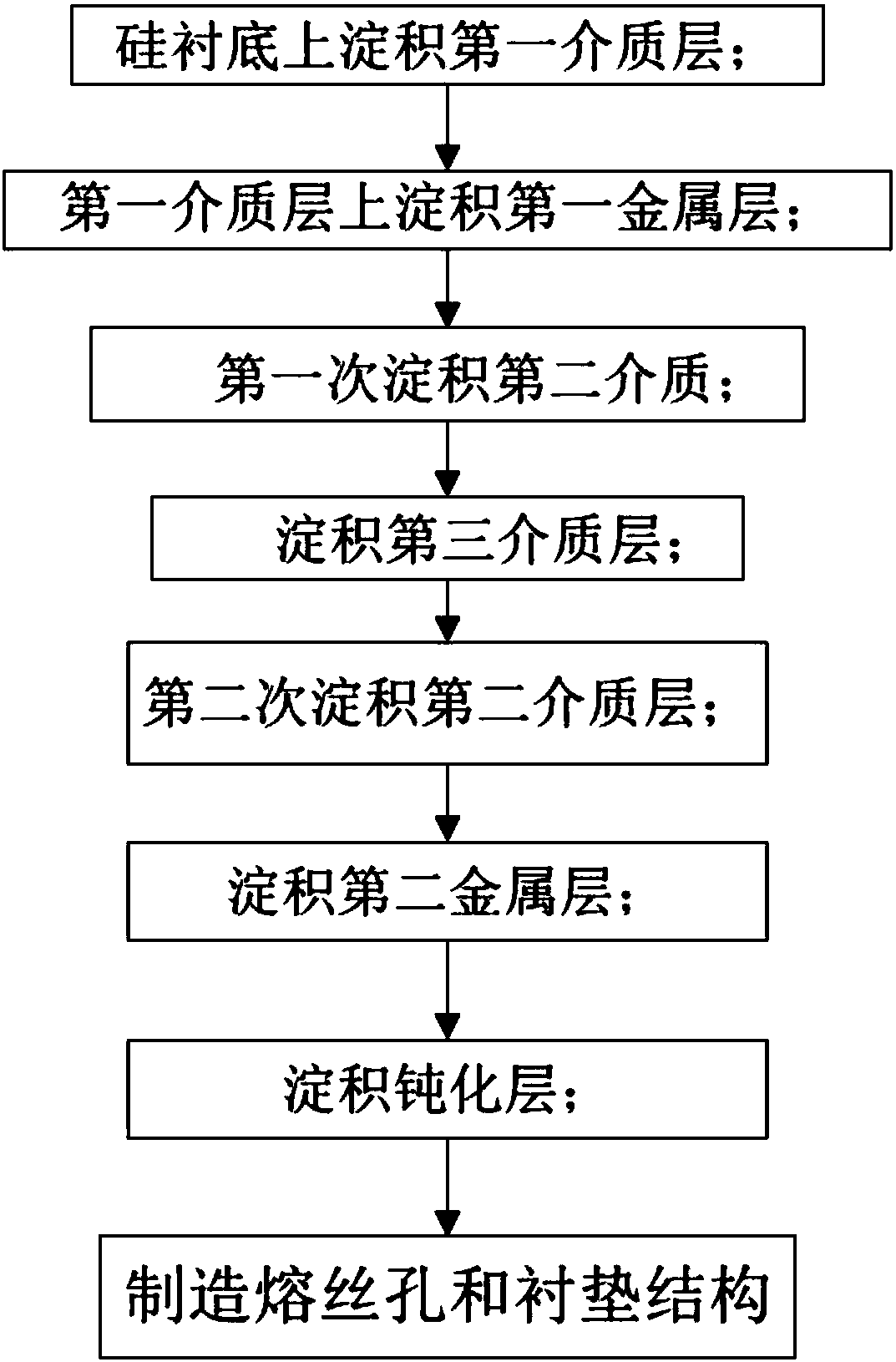
[0046] Such as image 3 As shown, the present invention provides a first embodiment of a semiconductor element fuse structure manufacturing method, including the following steps:
[0047] 1) Depositing a first dielectric layer on the silicon substrate;
[0048] 2) Depositing a first metal layer on the first dielectric layer;
[0049] 3) depositing a second dielectric layer on the second metal layer for the first time;
[0050] 4) depositing a third dielectric layer on the first deposited second dielectric layer;
[0051] 5) depositing a second dielectric layer on the third dielectric layer for the second time;
[0052] 6) depositing a second metal layer on the second dielectric layer deposited for the second time;
[0053] 7) depositing a passivation layer on the second metal layer and the second dielectric layer deposited for the second time;
[0054] 8) Apply photoresist on the passivation layer, and form a fuse hole by photolithography, and the fuse hole passes through...
no. 2 example
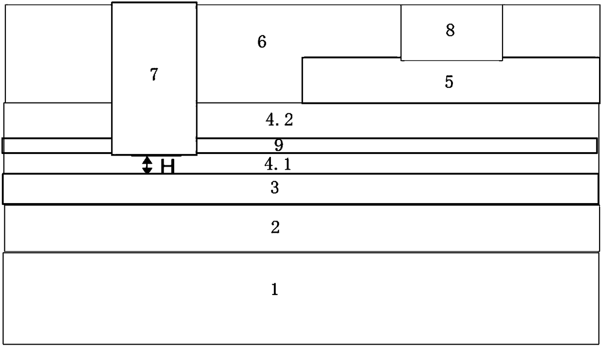
[0056] The present invention provides a second embodiment of a semiconductor element fuse structure manufacturing method, including the following steps:
[0057] 1) Depositing a first dielectric layer on the silicon substrate;
[0058] 2) Depositing a first metal layer on the first dielectric layer;
[0059] 3) Depositing a second dielectric layer for the first time on the second metal layer, the thickness of the second dielectric layer deposited for the first time is the tolerance thickness of the semiconductor element design;
[0060] 4) depositing a third dielectric layer on the first deposited second dielectric layer;
[0061] 5) depositing a second dielectric layer on the third dielectric layer for the second time;
[0062] 6) depositing a second metal layer on the second dielectric layer deposited for the second time;
[0063] 7) depositing a passivation layer on the second metal layer and the second dielectric layer deposited for the second time;
[0064] 8) Apply pho...
no. 3 example
[0066] The present invention provides a third embodiment of a method for manufacturing a fuse structure of a semiconductor element, which includes the following steps:
[0067] 1) Depositing a first dielectric layer on the silicon substrate;
[0068] 2) Depositing a first metal layer on the first dielectric layer;
[0069] 3) Depositing a second dielectric layer for the first time on the second metal layer, the thickness of the second dielectric layer deposited for the first time is the tolerance thickness of the semiconductor element design;
[0070] 4) Deposit the third dielectric layer on the second dielectric layer deposited for the first time, and deposit the third dielectric layer with a thickness of or
[0071] 5) depositing a second dielectric layer on the third dielectric layer for the second time;
[0072] 6) depositing a second metal layer on the second dielectric layer deposited for the second time;
[0073] 7) depositing a passivation layer on the second ...
PUM
 Abstract
Description
Claims
Application Information