Semiconductor structures and methods of forming them

A semiconductor and patterning technology, used in semiconductor devices, semiconductor/solid-state device manufacturing, electrical components, etc., and can solve problems such as poor target pattern quality

Active Publication Date: 2021-05-04
SEMICON MFG INT (SHANGHAI) CORP +1
View PDF4 Cites 0 Cited by
  • Summary
  • Abstract
  • Description
  • Claims
  • Application Information

AI Technical Summary

Problems solved by technology

[0004] However, even with the introduction of the self-aligned double patterning process, the quality of the target pattern formed after etching is still poor

Method used


Image

  • Semiconductor structures and methods of forming them
  • Semiconductor structures and methods of forming them
  • Semiconductor structures and methods of forming them

Examples


Embodiment Construction

[0016] It can be seen from the background art that even if a self-aligned double patterning process is introduced, the quality of the target pattern formed after etching is still poor, which easily leads to a decrease in the performance and yield of the formed semiconductor structure. The reason is analyzed in conjunction with an inventive method for forming a semiconductor structure.

[0017] refer to Figure 1 to Figure 5 , shows a schematic structural diagram corresponding to each step in a method for forming a semiconductor structure.

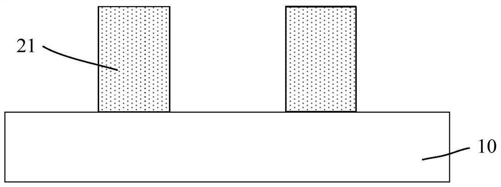
[0018] refer to figure 1 , providing a material layer 10 to be etched, and a plurality of discrete core layers 21 are formed on the material layer 10 to be etched.

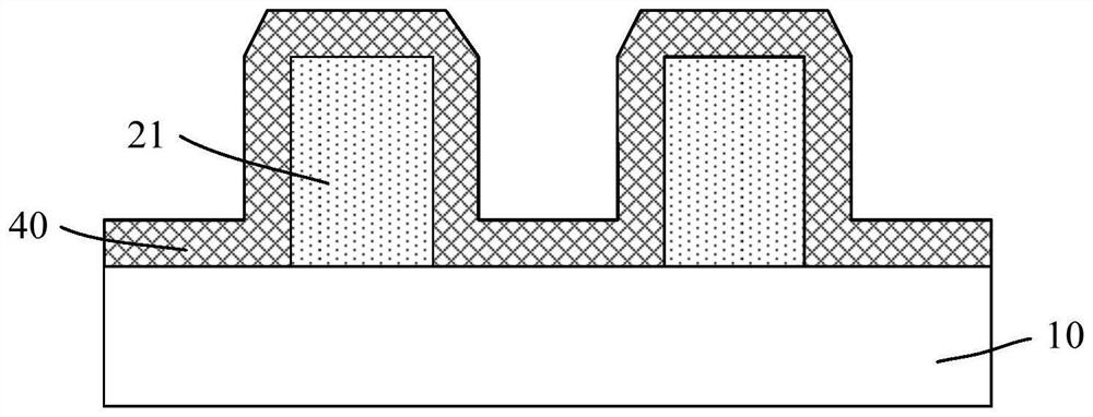
[0019] refer to figure 2 , forming a sidewall film 40 on the top and sidewall surfaces of the core layer 21 and the material layer 10 to be etched.

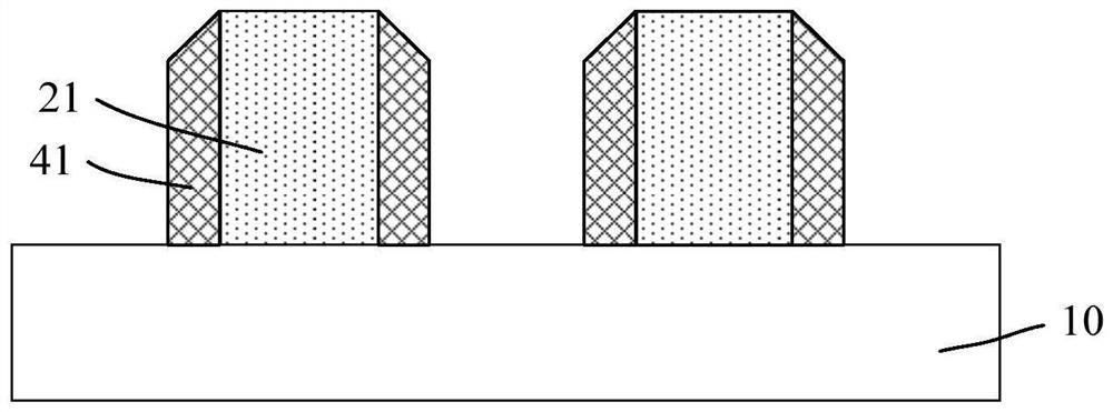
[0020] refer to image 3 , using a maskless etching process to etch the sidewall film 40 (such as figure 2 ), remove the...


PUM

PropertyMeasurementUnit
thicknessaaaaaaaaaa
thicknessaaaaaaaaaa

Abstract

A semiconductor structure and a forming method thereof, the method comprising: providing a material layer to be etched; forming a patterned core layer on the material layer to be etched; forming a sidewall on the top and side walls of the core layer and the material layer to be etched Wall film; carry out at least one top treatment on the side wall film, remove the side wall film higher than the top of the core layer, keep the side wall film on the side wall of the core layer as the first part of the side wall layer, and keep the side wall film on the material layer to be etched The wall film is used as the second part of the side wall layer; the steps of top treatment include: forming a sacrificial layer on the side wall film covering the surface of the wall film on the side wall of the core layer and the top; removing the sacrificial layer higher than the top of the core layer and Part-thickness or full-thickness sidewall film; removal of remaining sacrificial layer; removal of core layer; after removal of core layer, removal of second portion of sidewall layer. The morphology of the first part of the sidewall layer in the present invention is symmetrical, and after the material layer to be etched is etched using the first part of the sidewall layer as a mask, a target pattern with a better shape can be obtained.

Description

technical field [0001] The invention relates to the field of semiconductors, in particular to a semiconductor structure and a forming method thereof. Background technique [0002] Semiconductor technology continues to move towards smaller process nodes driven by Moore's Law. With the continuous advancement of semiconductor technology, the functions of devices are becoming more and more powerful, but the difficulty of semiconductor manufacturing is also increasing day by day. Photolithography technology is the most critical production technology in the semiconductor manufacturing process. With the continuous reduction of semiconductor process nodes, the existing light source lithography technology can no longer meet the needs of semiconductor manufacturing. Extreme ultraviolet lithography (EUV), multi- Beamless maskless technology and nanoimprint technology have become the research hotspots of next-generation lithography candidate technologies. However, the above-mentioned ...

Claims


Application Information

Patent Timeline
Patent Type & Authority Patents(China)
IPC IPC(8): H01L29/78H01L21/336
CPCH01L29/66795H01L29/785
Inventor 张冬平
Owner SEMICON MFG INT (SHANGHAI) CORP
Why Eureka
Try Eureka