

Semiconductor structure and formation method thereof
A semiconductor and patterning technology, used in semiconductor devices, semiconductor/solid-state device manufacturing, electrical components, etc., and can solve problems such as poor quality of target graphics
- Summary
- Abstract
- Description
- Claims
- Application Information
AI Technical Summary
Problems solved by technology
Method used
Image

Examples
Embodiment Construction
[0016] It can be known from the background art that even if the self-aligned double patterning process is introduced, the quality of the target pattern formed after etching is still poor, which easily leads to a decrease in the performance and yield of the formed semiconductor structure. The reasons for this are now analyzed in conjunction with a method for forming a semiconductor structure of the invention.
[0017] refer to Figure 1 to Figure 5 , a schematic diagram of the structure corresponding to each step in a method for forming a semiconductor structure is shown.
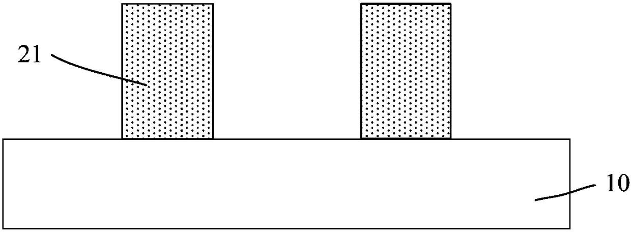
[0018] refer to figure 1 , to provide a material layer 10 to be etched, and a plurality of discrete core layers 21 are formed on the material layer 10 to be etched.
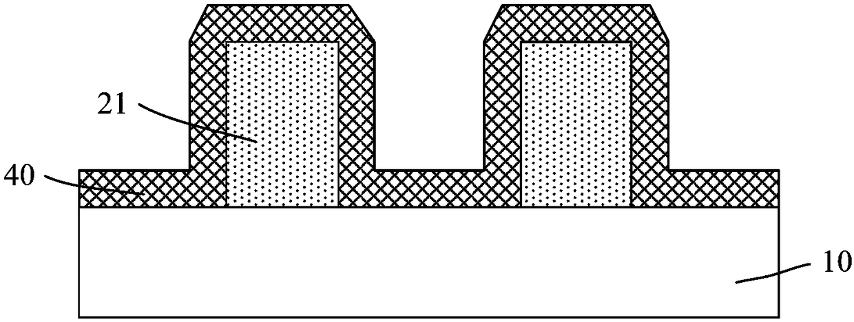
[0019] refer to figure 2 , forming a sidewall film 40 on the top and sidewall surfaces of the core layer 21 and the material layer 10 to be etched.
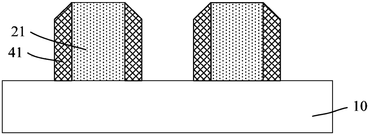
[0020] refer to image 3 , using a maskless etching process to etch the sidewall film 40...
PUM
 Abstract
Description
Claims
Application Information