Method and system to detect chippings on solar wafer

A technology for solar wafers and gaps is applied in the field of detecting gaps on the chamfered sidewalls of solar wafers, and can solve problems such as failure to detect gaps.

Active Publication Date: 2018-09-28
APPLIED MATERIALS INC
View PDF11 Cites 2 Cited by
  • Summary
  • Abstract
  • Description
  • Claims
  • Application Information

AI Technical Summary

Problems solved by technology

Currently, the camera cannot detect...

Method used


Image

  • Method and system to detect chippings on solar wafer
  • Method and system to detect chippings on solar wafer
  • Method and system to detect chippings on solar wafer

Examples


Embodiment Construction

[0047] Embodiments of the present invention described below relate to methods and systems for instantaneous detection of chips on chamfered sidewalls of solar wafers, with reference to the accompanying drawings.

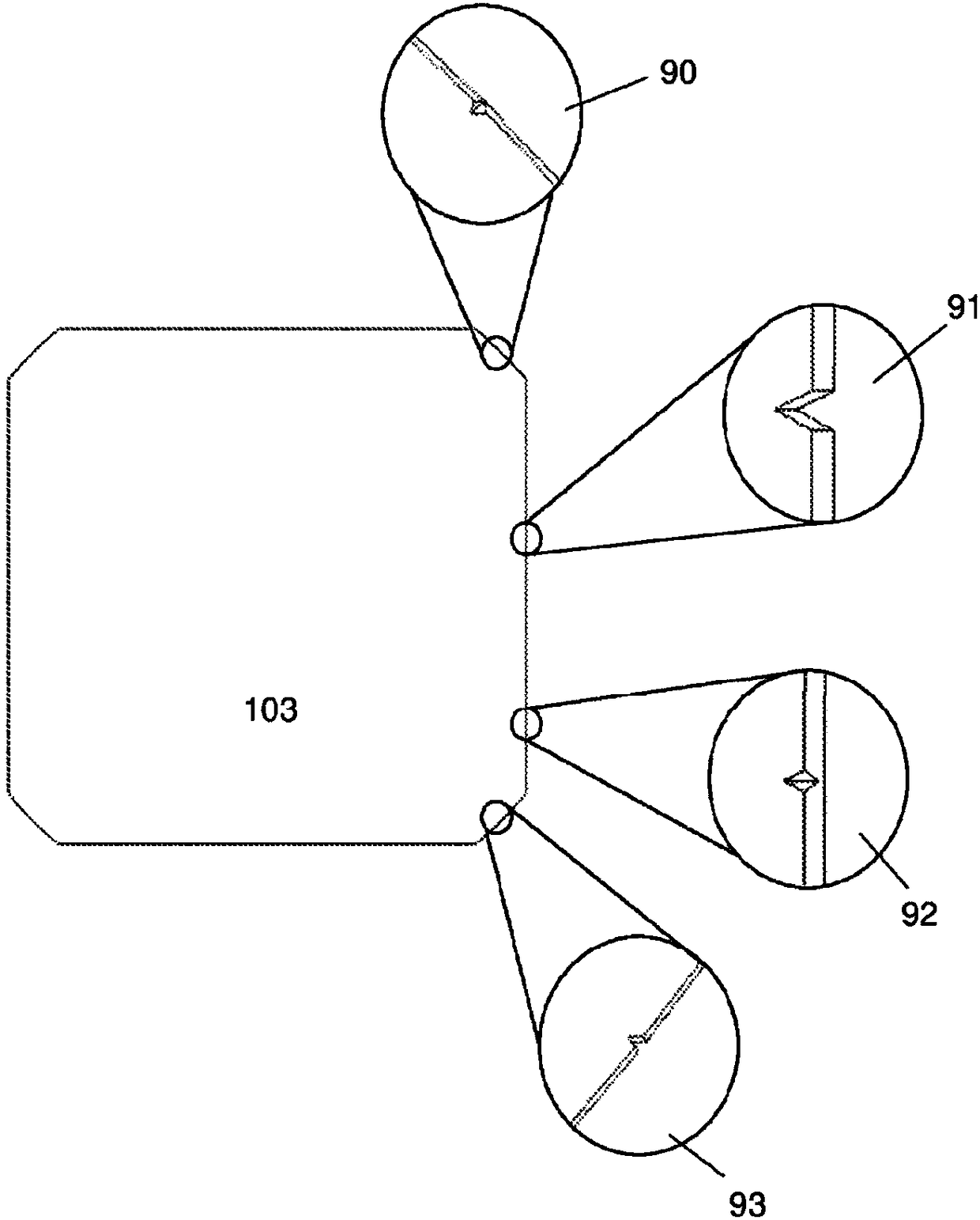
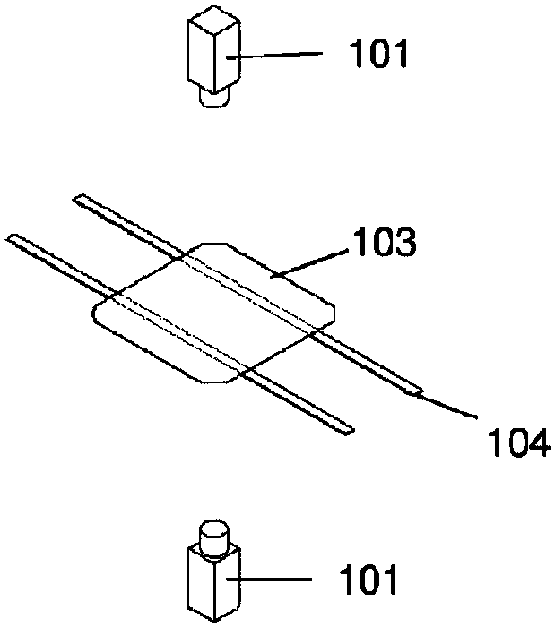
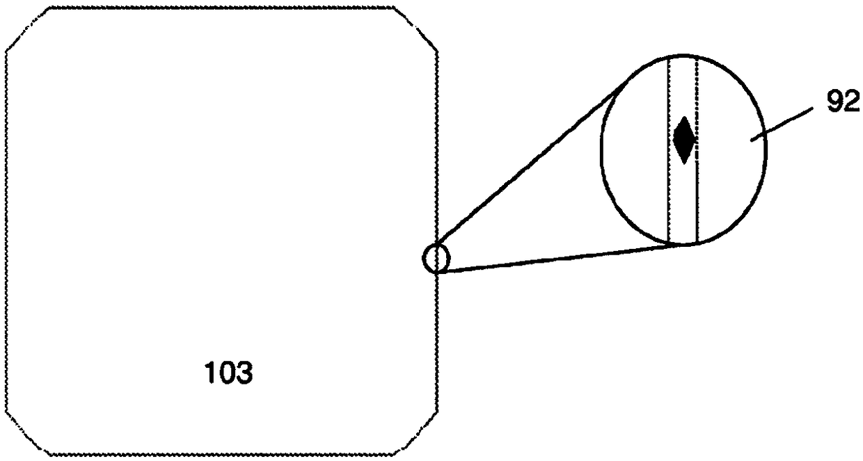
[0048] as the picture shows, figure 1 Schematic illustration of a gap formed in a solar wafer during the manufacture of a solar cell. These common defects include nicks on the top and bottom surfaces 93 along the chamfered edge, nicks on the top or bottom surface only along the straight edge 92 of the solar wafer, nicks on the top surface along the straight edge 91 of the solar wafer and a notch on the bottom surface, and a notch on the top or bottom surface along the chamfered edge 90 of the solar wafer. Figure 2-4 A notch formed on the solar wafer but not on the beveled edge is shown. In the drawings, reference numeral 101 denotes a camera, 103 denotes a solar wafer, and a conveyor belt is labeled 104 .

[0049] refer to Figure 5 , shows the notch formed in t...


PUM


Abstract

A chipping defect detection system for detecting a chipping defect at chamfer edge of a solar wafer, said solar wafer being substantially regular or square shape having straight edge and chamber edge,comprising: (a) a plurality of imaging means for pickup images of the position of the solar wafer and being positioned horizontally to the focusing plane of the solar wafer; (b) a plurality of illumination means to provide light for the imaging means while in operation thereof; (c) a conveyor belt for transporting the solar wafer horizontally in the course of chipping detection operation; (d) a sensing means providing a signal to trigger the imaging means to start an image capture; and (e) a strobe light driver which is triggered by the imaging means to drive the illumination means such thatthe imaging means provides an exposure time which coincides with the illumination means, thereby the chamfer edges are located at the out-of-focus position at the same position being sensed by the sensing means, and the image captured by the imaging means being not sharp is the chipping on the chamfer edges of the solar wafer. The present invention also discloses a method of chipping defect detection on a solar wafer.

Description

technical field [0001] The present invention relates to a system and method for detecting chipping on the chamfered sidewall of a solar wafer, and more particularly to a chipping detection system and method suitable for detecting chipping on any edge of a solar wafer that may cause cracks and chip breakage . Background technique [0002] Solar cell manufacturers often perform inspection of solar wafers as part of the solar cell manufacturing process. This is to ensure that any defects on the solar wafers are identified in the initial stages and that the subsequently produced solar wafers are of high quality. [0003] Solar wafers are extremely thin silicon wafers commonly used to make solar cells. In the manufacture of solar cells, solar wafers undergo a number of processes, such as deposition, etching, and patterning, etc., to serve as substrates for solar cells before they become functional solar cells during the manufacturing process. Due to the brittle nature of solar...

Claims


Application Information

Patent Timeline
IPC IPC(8): H02S50/10G01N21/95G01N21/88G01N21/892
CPCG01N21/88G01N21/892G01N21/95G01N21/9501H02S50/10H02S50/15Y02E10/50
Inventor 韩白权
Owner APPLIED MATERIALS INC
Why Eureka
Try Eureka