Method and system for implementing data protection of non-volatile memory chip
A non-volatile memory and data protection technology, applied in the field of storage systems, can solve problems such as data loss, and achieve the effects of short stay time, reliable design principles, and wide application prospects
- Summary
- Abstract
- Description
- Claims
- Application Information
AI Technical Summary
Problems solved by technology
Method used
Image
Examples
Embodiment 1
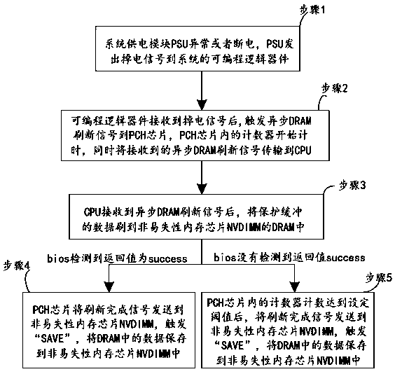
[0039] Such as figure 1 , figure 2 As shown, a method for realizing data protection of a non-volatile memory chip comprises the following steps:
[0040] Step 1: The PSU of the system power supply module is abnormal or powered off, and the PSU sends a power-off signal AC_Fail
[0041] to the programmable logic device of the system;
[0042] Step 2: After the programmable logic device receives the power-down signal AC_Fail, it triggers the asynchronous DRAM
[0043] The refresh signal ADR_Trigger# is sent to the PCH chip, the counter in the PCH chip starts timing, and the PCH chip transmits the received asynchronous DRAM refresh signal to the CPU through the power management synchronization signal PM_SYNC;
[0044] Step 3: After the CPU receives the refresh signal, refresh the data of the protection buffer ADR protected buffers to the DRAM of the non-volatile memory chip NVDIMM;
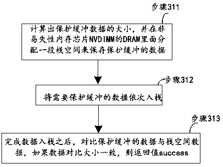
[0045] Step 31: After the CPU receives the refresh signal, it uses the rest of the filter cap...
Embodiment 2
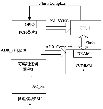
[0056] Such as image 3 As shown, a system for realizing data protection of a non-volatile memory chip includes a CPU 1 and a PCH chip 2, and the CPU 1 is connected to the PCH chip 2;
[0057] The PCH chip 2 is connected with a non-volatile memory chip NVDIMM 5, and the non-volatile memory chip NVDIMM5 is provided with a DRAM, and the CPU1 is connected with the DRAM;
[0058] The PCH chip 2 is also connected to a programmable logic device 3 , and the programmable logic device 3 is connected to a power supply module PSU 4 .
[0059] PCH chip 2 is connected to CPU1 through PM_SYNC signal;
[0060] A GPIO interface is defined on the PCH chip 1 for receiving the refresh completion signal, and the GPIO interface of the PCH chip 2 is connected to the CPU1.
Embodiment 3
[0062] A system for realizing data protection of a non-volatile memory chip, comprising a CPU 1 and a PCH chip 2, the CPU 1 being connected to the PCH chip 2;
[0063] The PCH chip 2 is connected with a non-volatile memory chip NVDIMM 5, and the non-volatile memory chip NVDIMM5 is provided with a DRAM, and the CPU1 is connected with the DRAM;
[0064] The PCH chip 2 is also connected to a programmable logic device 3 , and the programmable logic device 3 is connected to a power supply module PSU 4 .
[0065] PCH chip 2 is connected to CPU1 through PM_SYNC signal;
[0066] A GPIO interface is defined on the PCH chip 1 for receiving the refresh completion signal, and the GPIO interface of the PCH chip 2 is connected to the CPU1; the programmable logic device 3 is a CPLD chip.
[0067] A method for realizing non-volatile memory chip data protection based on the above system, comprising the steps of:
[0068] Step 1: The PSU of the system power supply module is abnormal or powere...
PUM
 Abstract
Description
Claims
Application Information


