Heterojunction photoelectric sensor and preparation method thereof

A photoelectric sensor and heterojunction technology, applied in circuits, electrical components, semiconductor devices, etc., can solve the problem of poor response sensitivity of photoelectric sensors, and achieve the effect of improving response sensitivity, strong detection ability, and wide detection range

Active Publication Date: 2018-10-16
SHENZHEN UNIV
View PDF9 Cites 9 Cited by
  • Summary
  • Abstract
  • Description
  • Claims
  • Application Information

AI Technical Summary

Problems solved by technology

[0005] In view of the above-mentioned deficiencies in the prior art, the object of the present invention is to provide a heterojunction photoelectric sensor and its preparation method, aiming to solve the problem of poor response sensitivity of the existing photoelectric sensor

Method used


Image

  • Heterojunction photoelectric sensor and preparation method thereof
  • Heterojunction photoelectric sensor and preparation method thereof
  • Heterojunction photoelectric sensor and preparation method thereof

Examples


Embodiment Construction

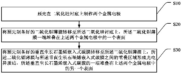
[0034] The present invention provides a heterojunction photoelectric sensor and its preparation method. In order to make the purpose, technical solution and effect of the present invention clearer and clearer, the present invention will be further described in detail below. It should be understood that the specific embodiments described here are only used to explain the present invention, not to limit the present invention.

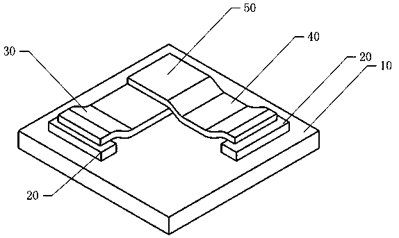
[0035] see figure 1 , figure 1 It is a structural schematic diagram of a preferred embodiment of a heterojunction photoelectric sensor of the present invention. As shown in the figure, the heterojunction photoelectric sensor includes a substrate 10, two metal electrodes 20 fixedly arranged on the substrate 10, and The molybdenum disulfide thin film 30 and the vertically grown graphene-embedded carbon film 40 stacked on the substrate 10 are provided with a partial overlapping region between the molybdenum disulfide thin film 30 and the vertically grown gr...


PUM

PropertyMeasurementUnit
thicknessaaaaaaaaaa

Abstract

The invention discloses a heterojunction photoelectric sensor and a preparation method thereof. The photoelectric sensor comprises a substrate, two metal electrodes fixedly arranged on the substrate,and a molybdenum disulfide thin film and a vertical growth graphene embedded carbon film which are stacked on the substrate, wherein a partially overlapped region is arranged between the molybdenum disulfide thin film and the vertical growth graphene embedded carbon film; photoelectric heterojunctions are formed in the partially overlapped region through Van der Waals interaction; and the two non-overlapping ends of the molybdenum disulfide thin film and the vertical growth graphene embedded carbon film are respectively stacked on the surfaces of the two metal electrodes. The photoelectric heterojunctions formed by stacking the molybdenum disulfide thin film and the vertical growth graphene embedded carbon film can effectively promote the response sensitivity of the photoelectric sensor, and the photoelectric sensor is wider in detection range and higher in detection capacity.

Description

technical field [0001] The invention relates to the field of photoelectric sensors, in particular to a heterojunction photoelectric sensor and a preparation method thereof. Background technique [0002] A photodetector is a device that can convert real-time optical signals into real-time electrical signals, and it plays an important role in optoelectronic systems. Photodetectors are used in a wide range of applications in technology, business, and various fields. Today's photodetectors are divided into photon detectors and thermal detectors, among which photon detectors are the mainstream, and photoelectric detectors based on graphene-like two-dimensional materials (silicon, germanium, transition metal chalcogenides, etc.) Detector development has entered the mainstream. [0003] Since the discovery of graphene, two-dimensional materials with graphene structure and graphene-like structure (black scale, molybdenum disulfide, etc.) have become the mainstream of optoelectroni...

Claims


Application Information

Patent Timeline
Patent Type & Authority Applications(China)
IPC IPC(8): H01L31/0352H01L31/028H01L31/032H01L31/109H01L31/18
CPCH01L31/028H01L31/032H01L31/035281H01L31/109H01L31/18Y02P70/50
Inventor 张希陈泽宇陈文聪刁东风
Owner SHENZHEN UNIV
Why Eureka
Try Eureka