
Manufacturing method for display panel

A technology for a display panel and a manufacturing method, which is applied to the photoengraving process, optics, optomechanical equipment and other directions of the pattern surface, can solve the problems of identification interference, the inability of the exposure machine to be accurately aligned, and the influence of the black matrix shading effect, etc., and achieve accurate The effect of recognition

Inactive Publication Date: 2018-10-19
HKC CORP LTD
View PDF8 Cites 9 Cited by
  • Summary
  • Abstract
  • Description
  • Claims
  • Application Information

AI Technical Summary

Problems solved by technology

[0003] However, due to the high optical density (optical density, OD) of the black light-shielding layer material forming the black matrix, after the black light-shielding material is coated, it will interfere with the recognition of the mask exposure alignment mark, which will cause the exposure machine to fail. Precise alignment; if a black light-shielding layer material with a low optical density value is used, although it can reduce the difficulty of identifying the mark, it will seriously affect the light-shielding effect of the black matrix

Method used


Image

  • Manufacturing method for display panel
  • Manufacturing method for display panel
  • Manufacturing method for display panel

Examples


Embodiment Construction

[0036] In order to make the purpose, technical solutions and advantages of the present invention clearer, the technical solutions of the present invention will be clearly and completely described through implementation with reference to the accompanying drawings in the embodiments of the present invention. Obviously, the described embodiments are the embodiment of the present invention. Some, but not all, embodiments. Based on the embodiments of the present invention, all other embodiments obtained by persons of ordinary skill in the art without making creative efforts belong to the protection scope of the present invention.

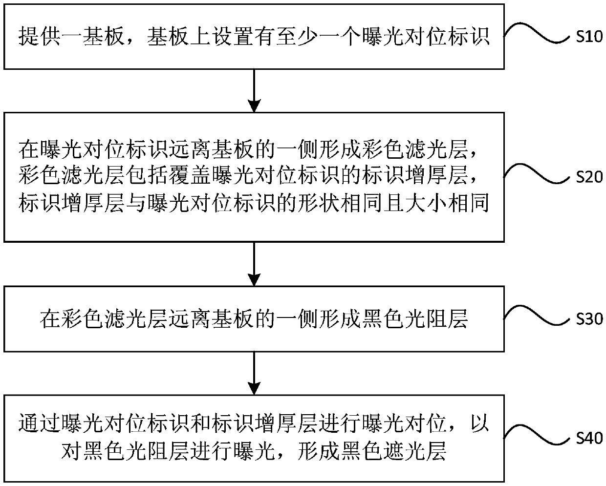
[0037] figure 1 It is a schematic flowchart of a manufacturing method of a display panel provided by an embodiment of the present invention. refer to figure 1 , the method includes:

[0038] S10 , providing a substrate, on which at least one exposure alignment mark is disposed.

[0039] Wherein, the substrate includes a display area and a non-display...


PUM


Abstract

The embodiment of the invention discloses a manufacturing method for a display panel. The method comprises the following steps that a substrate is provided, and at least one exposure alignment identification is arranged on the substrate; a colorful filter layer is formed at one side, away from the substrate, of the at least one exposure alignment identification, the colorful filter layer comprisesan identification thickening layer covering the exposure alignment identification, and shapes and sizes of the identification thickening layer and exposure alignment identification are same; a blacklight resistance layer is formed at one side, away from the substrate, of the colorful filter layer; exposure alignment is conducted by utilizing the exposure alignment identification and the identification thickening layer so as to carry out exposure on the black light resistance layer, and a block light shading layer is formed. According to the provided manufacturing method for the display panel, the identification thickening layer covering the exposure alignment identification is formed to increase the height of the position of the exposure alignment identification, and after the subsequentblack light resistance layer is formed, the exposure alignment identification can be accurately identified, therefore the manufacturing accuracy of the black shading layer is improved.

Description

technical field [0001] Embodiments of the present invention relate to display technologies, and in particular to a method for manufacturing a display panel. Background technique [0002] With the development of display technology, in order to avoid the mismatch of light-shielding areas caused by the dislocation of the upper and lower substrates, the black matrix is ​​usually integrated on the array substrate, that is, BOA (Black Matrix on Array) technology. At the same time, in the manufacturing process of the display device, in order to improve the alignment accuracy in the manufacturing process, an exposure alignment mark is usually provided. [0003] However, due to the high optical density (optical density, OD) of the black light-shielding layer material forming the black matrix, after the black light-shielding material is coated, it will interfere with the recognition of the mask exposure alignment mark, which will cause the exposure machine to fail. Precise alignment;...

Claims


Application Information

Patent Timeline
Patent Type & Authority Applications(China)
IPC IPC(8): G02F1/1335
CPCG02F1/133512G02F1/133514G02F1/133516G03F7/0007G02F1/133354
Inventor 黄北洲
Owner HKC CORP LTD
Learn More