

Nonspecific adsorption prevention three-dimensional chip and application thereof
A three-dimensional chip, non-specific technology, applied in laboratory containers, measuring devices, material analysis through optical means, etc., can solve the problem of "pollution" on the surface of sensor chips, achieve good suppression effect, and have scientific and reasonable structural design , The effect of simple preparation steps
- Summary
- Abstract
- Description
- Claims
- Application Information
AI Technical Summary
Benefits of technology
Problems solved by technology
Method used
Image

Examples
Embodiment 1
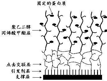
[0053] An anti-nonspecific adsorption three-dimensional chip, prepared by the following method:
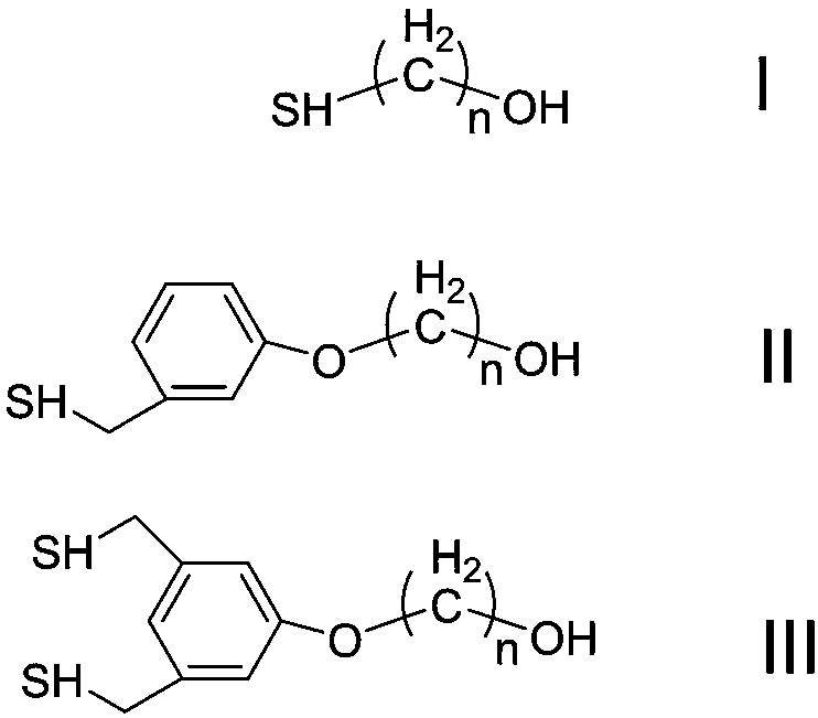
[0054]1) Magnetron sputtering thickness is 1nm chrome film on clean glass substrate surface, subsequently, the gold film that thickness is about 30nm is magnetron sputtered on the surface of chrome film; Clean above-mentioned plated gold film with plasma cleaner Glass substrate, removes its pollutant that is adsorbed on the surface; The glass substrate coated with gold film after cleaning is soaked in the ethanol solution that contains the diluent (formula I) and initiator (formula I) that total concentration is 1mM immediately , wherein the molar ratio of the initiator to the diluent is 1:1000, the diluent and the initiator are self-assembled on the gold surface through the Au-S bond; after 5 hours of reaction, the glass substrate surface self-assembles with a single-layer initiator Floor.
[0055] 2) Under a protective gas atmosphere, add 1 mole part of alkynyl group-containing...
Embodiment 2
[0058] An anti-nonspecific adsorption three-dimensional chip, prepared by the following method:
[0059] 1) Magnetron sputtering thickness is 5nm chrome film on clean glass substrate surface, subsequently, the gold film that thickness is about 50nm is magnetron sputtered on the surface of chrome film; Clean above-mentioned plated gold film with plasma cleaner Glass substrate, remove its pollutant that is adsorbed on the surface; The glass substrate coated with gold film after cleaning is soaked in the ethanol solution that contains the diluent (formula II) and initiator (formula II) that total concentration is 1mM immediately , wherein the molar ratio of the initiator to the diluent is 100:1000, the diluent and the initiator are self-assembled on the gold surface through the Au-S bond; after 10 hours of reaction, the glass substrate surface is self-assembled with a monolayer structure Floor.
[0060] 2) Under a protective gas atmosphere, add 1 mole part of azide group-contain...
Embodiment 3
[0063] An anti-nonspecific adsorption three-dimensional chip, prepared by the following method:
[0064] 1) Magnetron sputtering thickness is 3nm chrome film on clean glass substrate surface, subsequently, the gold film that thickness is about 40nm is magnetron sputtered on the surface of chrome film; Clean above-mentioned plated gold film with plasma cleaner Glass substrate, removes its pollutant that is adsorbed on the surface; The glass substrate coated with gold film after cleaning is soaked in the ethanol solution that contains the diluent (formula III) and initiator (formula III) that total concentration is 1mM immediately , wherein the molar ratio of the initiator to the diluent is 20:1000, the diluent and the initiator are self-assembled on the gold surface through the Au-S bond; after 12 hours of reaction, the glass substrate surface is self-assembled with a single-layer initiator Floor.
[0065] 2) Under a protective gas atmosphere, add 1 mole part of alkynyl group-...
PUM
 Abstract
Description
Claims
Application Information