Trench gate super junction device and manufacturing method thereof

A technology of super junction devices and manufacturing methods, which is applied in the manufacture of trench gate super junction devices and the field of trench gate super junction devices, can solve the problems of cost increase and unfavorable device size reduction, and achieve cost saving and size reduction Effect

Active Publication Date: 2018-11-13
SHANGHAI HUAHONG GRACE SEMICON MFG CORP
View PDF4 Cites 0 Cited by
  • Summary
  • Abstract
  • Description
  • Claims
  • Application Information

AI Technical Summary

Problems solved by technology

The use of photolithography will increase the cost and is not conducive to the reduction of the size of the device

Method used


Image

  • Trench gate super junction device and manufacturing method thereof
  • Trench gate super junction device and manufacturing method thereof
  • Trench gate super junction device and manufacturing method thereof

Examples


Embodiment Construction

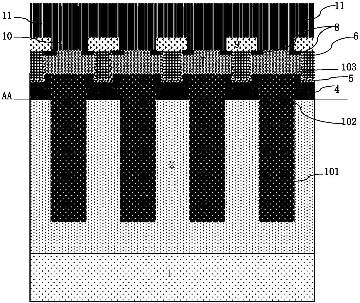
[0051] Such as figure 1As shown, it is a schematic structural diagram of a trench-gate super-junction device according to an embodiment of the present invention; the trench-gate super-junction device according to an embodiment of the present invention includes:

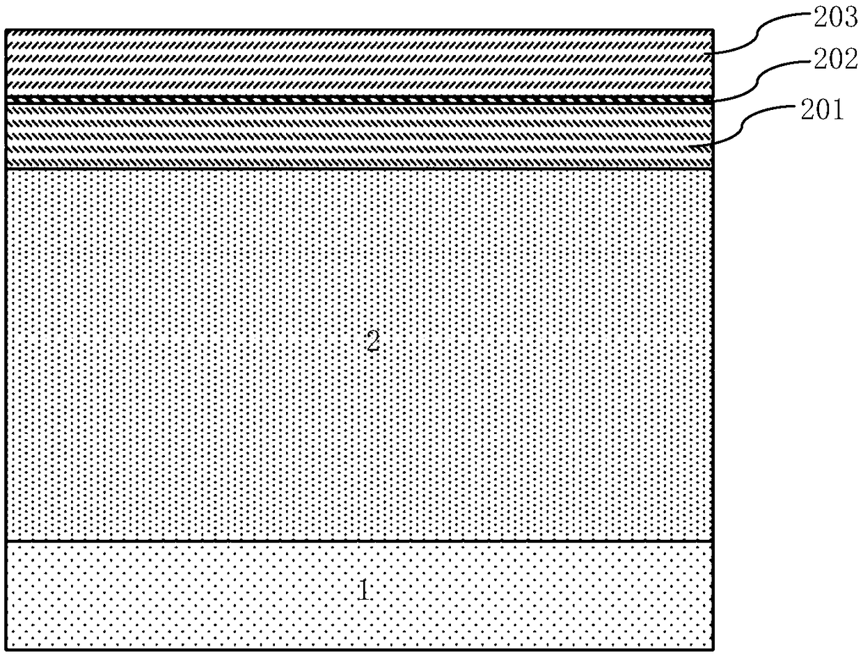
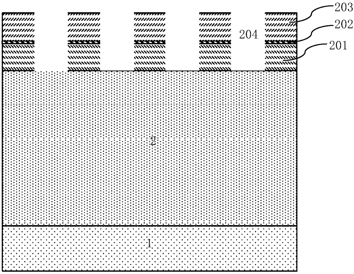
[0052] The super junction trench 101 is formed in the first N-type epitaxial layer 2; a hard mask layer is formed on the surface of the first N-type epitaxial layer 2, and the super junction trench 101 is formed by the hard mask The first opening 204 is defined by layer photolithography. For the first opening 204 please refer to Figure 2B shown.

[0053] The P-type epitaxial layer 3 is filled in the super junction trench 101 and the first opening 204 at the top to form a P-type thin layer 3 .

[0054] After the P-type thin layer 3 is formed, the hard mask layer is removed and the P-type protrusion structure of the P-type thin layer 3 is formed, and the P-type protrusion structure is filled in the first opening 204...


PUM


Abstract

The invention discloses a trench gate super junction device. The device comprises super junction trenches defined by first openings formed by lithography etching of a hard mask layer, wherein the super junction trenches and the first openings at the top are filled with P-type epitaxial layers, and P-type thin layers are formed; the hard mask layer is removed, then, P-type bulge structures of the P-type thin layers are formed, regions among the P-type bulge structures are self-aligned to form top trenches; second N-type epitaxial layers are formed on side surfaces and bottom surfaces of the toptrenches and are self-aligned to define gate trenches of trench gates; gate dielectric layers and polysilicon gates are formed in the gate trenches; N-type thin layers are formed by stacking the first and second N-type epitaxial layers between the P-type thin layers, and super junctions are formed by alternating arrangement of the N-type thin layers and the P-type thin layers. The invention further discloses a manufacturing method of the trench gate super junction device. The trench gates can be defined by self-alignment, so that a trench gate mask can be saved, the cost can be saved, and thesize of the device is further reduced.

Description

technical field [0001] The invention relates to the field of semiconductor integrated circuit manufacturing, in particular to a trench gate super junction device; the invention also relates to a manufacturing method of the trench gate super junction device. Background technique [0002] The superjunction is composed of alternately arranged P-type thin layers, also called P-type pillars (Pillar) and N-type thin layers, also called N-type pillars, formed in a semiconductor substrate, and the matching is completed by using P-type thin layers and N-type thin layers The formed depletion layer improves the reverse withstand voltage while maintaining a small on-resistance. [0003] The super junction is usually formed by trench etching and trench epitaxial filling. First, a super junction trench is formed on the surface of the N-type epitaxial layer, and then a P-type epitaxial layer is filled in the super junction trench to form a P-type thin layer; N-type epitaxial layers betwee...

Claims


Application Information

Patent Timeline
Patent Type & Authority Applications(China)
IPC IPC(8): H01L29/423H01L29/78H01L21/336H01L29/06
CPCH01L29/0634H01L29/4236H01L29/42368H01L29/66666H01L29/7827
Inventor 李昊
Owner SHANGHAI HUAHONG GRACE SEMICON MFG CORP
Why Eureka
Try Eureka