Fabrication method of radio frequency ldmos device

A manufacturing method and device technology, applied in semiconductor/solid-state device manufacturing, semiconductor devices, electrical components, etc., to achieve low cost, small size, and eliminate registration problems

Active Publication Date: 2017-10-24
SHANGHAI HUAHONG GRACE SEMICON MFG CORP
View PDF3 Cites 0 Cited by
  • Summary
  • Abstract
  • Description
  • Claims
  • Application Information

AI Technical Summary

Problems solved by technology

This existing method self-aligns to define the silicide formation regions on top of the polysilicon gates, but requires an additional photolithography step to define the silicide formation regions for the source and drain regions

Method used


Image

  • Fabrication method of radio frequency ldmos device
  • Fabrication method of radio frequency ldmos device
  • Fabrication method of radio frequency ldmos device

Examples


Embodiment Construction

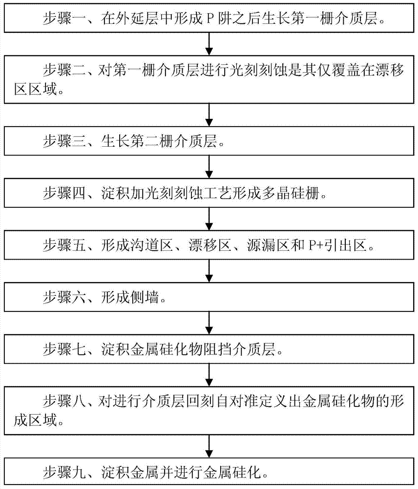
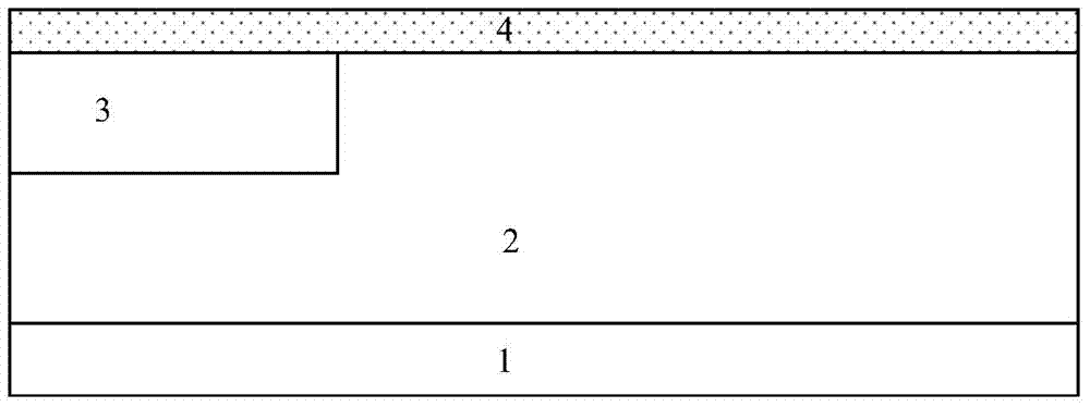
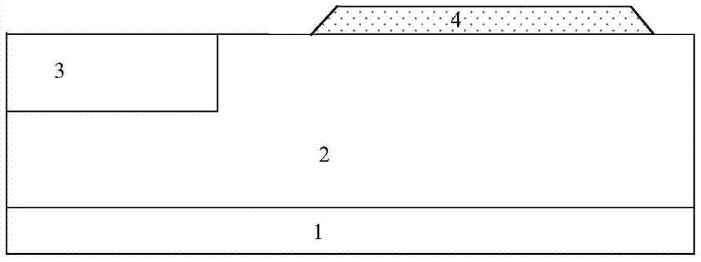
[0041] Such as figure 1 Shown is the flow chart of the manufacturing method of the radio frequency LDMOS device of the embodiment of the present invention; Figure 2A to Figure 2I Shown is a schematic diagram of the device structure in each step of the manufacturing method of the radio frequency LDMOS device of the embodiment of the present invention; the manufacturing method of the radio frequency LDMOS device of the embodiment of the present invention includes the following steps:

[0042] Step 1, such as Figure 2AAs shown, an epitaxial layer 2 is formed on the surface of a silicon substrate 1 , a P well 3 is formed in the epitaxial layer 2 , and then a first gate dielectric layer 4 is grown. In the embodiment of the present invention, the silicon substrate 1 is heavily doped with P type, and the epitaxial layer 2 is lightly doped with P type, and the epitaxial layer 2 can be formed by stacking multiple epitaxial layers.

[0043] The material of the first gate dielectric ...


PUM


Abstract

The invention discloses a manufacturing method of a radio frequency LDMOS device. The manufacturing method comprises the steps that after a trap P is formed in an epitaxial layer, a first gate dielectric layer grows; photoetching is carried out on the first gate dielectric layer so that the first gate dielectric layer can only cover a drift region; a second gate dielectric layer grows; a polysilicon gate is formed through the deposition and photoetching technology; a channel region, the drift region, a source region, a drain region and a P+ leading-out region are formed; a side wall is formed; a metal silicide barrier dielectric layer is deposited; repeated etching is carried out on the dielectric layers, and a metal silicide forming region is defined through self-alignment; metal silicification is carried out on the deposited metal. The metal silicide forming region of the device can be defined through self-alignment, and the coupling capacitance between a gate electrode and the drain electrode of the device can be reduced.

Description

technical field [0001] The invention relates to a method for manufacturing a semiconductor integrated circuit, in particular to a method for manufacturing a radio frequency LDMOS device. Background technique [0002] In order to improve the radio frequency performance of radio frequency lateral field effect transistor (RF LDMOS) with a breakdown voltage above 50V, it is necessary to reduce the parasitic capacitance and resistance. [0003] In the existing process, in order to reduce the gate resistance, a stack of polysilicon and metal silicide is used; metal silicide can be deposited together with polysilicon, such as tungsten silicon, but its resistance per square is generally above 5 ohms; the other is Depositing metals such as titanium (Ti) or cobalt (Co) can give a resistance of 2 ohms per square. [0004] Since the gate width of RFLDMOS is less than 0.5 microns, and in order to increase the breakdown voltage, the side of the polysilicon gate close to the drain end is ...

Claims


Application Information

Patent Timeline
Patent Type & Authority Patents(China)
IPC IPC(8): H01L21/336
CPCH01L21/28255H01L29/66681H01L29/66719
Inventor 王春蔡莹周正良
Owner SHANGHAI HUAHONG GRACE SEMICON MFG CORP
Why Eureka
Try Eureka