Manufacturing method of semiconductor device

A manufacturing method and semiconductor technology, applied in semiconductor/solid-state device manufacturing, semiconductor devices, electrical components, etc., can solve problems such as the influence of lithography alignment accuracy, Mesa width, etc.

Pending Publication Date: 2021-03-05
NANTONG SANRISE INTEGRATED CIRCUIT CO LTD
View PDF0 Cites 1 Cited by
  • Summary
  • Abstract
  • Description
  • Claims
  • Application Information

AI Technical Summary

Problems solved by technology

In addition, the position of the contact hole is also affected by the photolithographic alignment accuracy
This leads to a wider Mesa width

Method used


Image

  • Manufacturing method of semiconductor device
  • Manufacturing method of semiconductor device
  • Manufacturing method of semiconductor device

Examples


no. 1 example

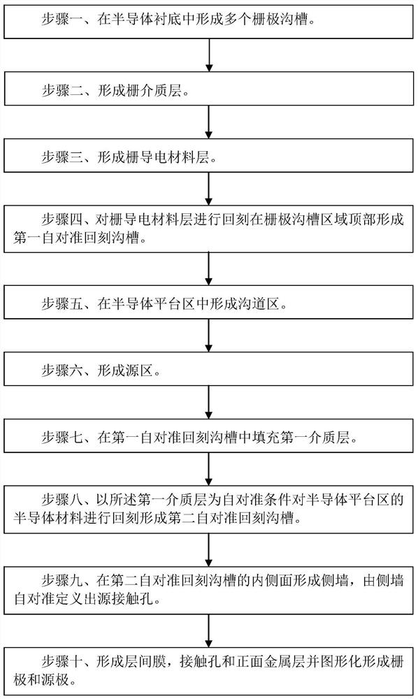
[0057] Such as figure 2 Shown is the flowchart of the manufacturing method of the semiconductor device of the first embodiment of the present invention; as Figure 3A to Figure 3I Shown is a schematic diagram of the device structure in each step of the manufacturing method of the semiconductor device according to the first embodiment of the present invention. The method for manufacturing a semiconductor device according to the first embodiment of the present invention includes the following steps:

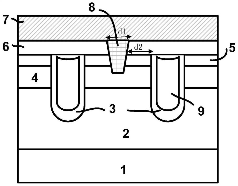
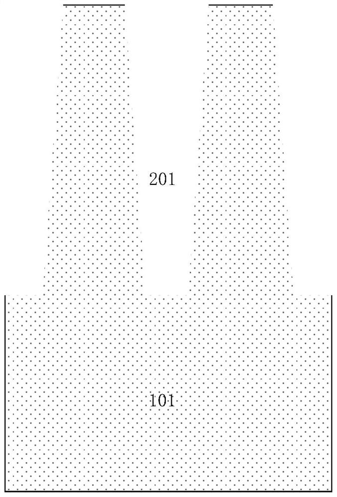
[0058] Step 1, such as Figure 3A As shown, a semiconductor substrate 101 is provided, and the top surface of the semiconductor substrate 101 is a first surface; a plurality of gate trenches 201 are formed in the semiconductor substrate 101 by photolithography definition and etching process, and each phase The area between the adjacent gate trenches 201 is a semiconductor platform region; in the current flow region of a semiconductor device, a primitive cell is composed of one g...

no. 1 example approach

[0092] Take a semiconductor device with a breakdown voltage of 20V and a cell step of 0.5 microns, that is, the corresponding MOSFET device in the first embodiment of the present invention, as an example: for a low-voltage MOSFET, a highly doped phosphorus semiconductor substrate 101 is usually used , instead of using a highly doped arsenic semiconductor substrate, because the phosphorus-doped semiconductor substrate has a lower minimum resistivity than the arsenic-doped semiconductor substrate. At present, the resistivity of phosphorus-doped semiconductor substrates can be as low as 0.7mΩ*cm to 0.9mΩ*cm, while for arsenic substrates, the resistivity can be as low as 1.0mΩ*cm to 1.5mΩ*cm. Because of the low specific on-resistance of low-voltage devices, the substrate accounts for a large proportion of the total on-resistance, and lower substrate resistance becomes more important.

[0093] There is an epitaxial layer on the semiconductor substrate 101. In order to reduce the re...


PUM

PropertyMeasurementUnit
electrical resistivityaaaaaaaaaa
thicknessaaaaaaaaaa
electrical resistivityaaaaaaaaaa

Abstract

The invention discloses a manufacturing method of a semiconductor device. The manufacturing method comprises the following steps: 1, forming a gate trench in a semiconductor substrate; 2, forming a gate dielectric layer; 3, forming a gate conductive material layer; 4, performing back etching on the gate conductive material layer to form a first self-aligned back etching trench at the top of the gate trench region; 5, forming a channel region; 6, forming a source region; 7, filling a first dielectric layer in the first self-alignment back-etching groove; 8, taking the first dielectric layer asa self-alignment condition to etch back the semiconductor material of the semiconductor platform region to form a second self-alignment etch-back trench; 9, forming a side wall for defining a source contact hole in a self-alignment manner on the inner side surface of the second self-alignment back-etching groove; 10, forming an interlayer film, a contact hole and a front metal layer, and patterning to form a grid electrode and a source electrode. According to the invention, the contact hole at the top of the source region can be self-aligned and defined, so that the stepping of the device canbe reduced and the specific on-resistance of the device can be reduced.

Description

technical field [0001] The invention relates to a method for manufacturing a semiconductor integrated circuit, in particular to a method for manufacturing a semiconductor device. Background technique [0002] Such as figure 1 As shown, it is a schematic structural diagram of an existing trench gate MOSFET device, including: a highly doped semiconductor substrate such as a silicon substrate 1, and the resistivity of the silicon substrate 1 is usually between 0.001Ω*cm and 0.002Ω*cm , the thickness of the silicon substrate 1 is also desired to be as thin as possible to reduce the substrate resistance. [0003] An epitaxial layer such as a silicon epitaxial layer 2 is formed on the surface of the silicon substrate 1 , and the thickness and doping concentration of the silicon epitaxial layer 2 determine the device voltage of the device. The higher the breakdown voltage of the device, the thicker the silicon epitaxial layer 2 needs to be, and the lower the doping concentration....

Claims


Application Information

Patent Timeline
Patent Type & Authority Applications(China)
IPC IPC(8): H01L29/78H01L21/336H01L29/423H01L21/768
CPCH01L21/76804H01L21/76805H01L21/76831H01L29/4236H01L29/66477H01L29/78
Inventor 曾大杰
Owner NANTONG SANRISE INTEGRATED CIRCUIT CO LTD
Why Eureka
Try Eureka