Trench gate MOSFET device and manufacturing method thereof

A trench gate and device technology, applied in the manufacture of trench gate MOSFET devices, in the field of trench gate MOSFET devices, can solve problems such as the influence of lithographic alignment accuracy and Mesa width

Active Publication Date: 2020-07-03
SHENZHEN SANRISE TECH CO LTD
View PDF7 Cites 4 Cited by
  • Summary
  • Abstract
  • Description
  • Claims
  • Application Information

AI Technical Summary

Problems solved by technology

In addition, the position of the contact hole is also affected by the photolithographic alignment accuracy
This leads to a wider Mesa width

Method used


Image

  • Trench gate MOSFET device and manufacturing method thereof
  • Trench gate MOSFET device and manufacturing method thereof
  • Trench gate MOSFET device and manufacturing method thereof

Examples


no. 1 example

[0064] Trench gate MOSFET device of the first embodiment of the present invention:

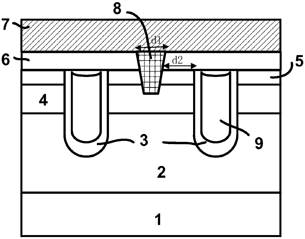
[0065] Such as figure 2 Shown is a schematic structural diagram of a trench gate MOSFET device in the first embodiment of the present invention. The trench gate MOSFET device in the first embodiment of the present invention is formed in a semiconductor substrate 101, and the top surface of the semiconductor substrate 101 is the first Surface: the current flow area of ​​the trench gate MOSFET device is composed of a plurality of primitive cells arranged periodically, and the trench gate of each primitive cell includes a gate trench 201 , a gate dielectric layer 102 and a gate conductive material layer 103 .

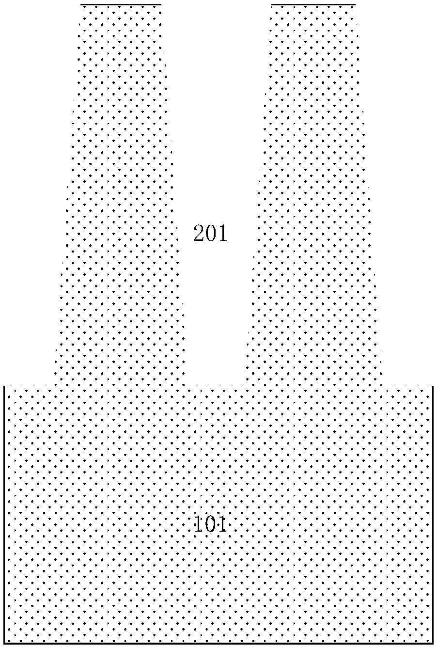
[0066] The gate trenches 201 are formed in the semiconductor substrate 101 , and the regions between adjacent gate trenches 201 are semiconductor platform regions.

[0067] The gate dielectric layer 102 is formed on the bottom surface and side surfaces of the gate trench 201 , and the ga...

no. 1 example

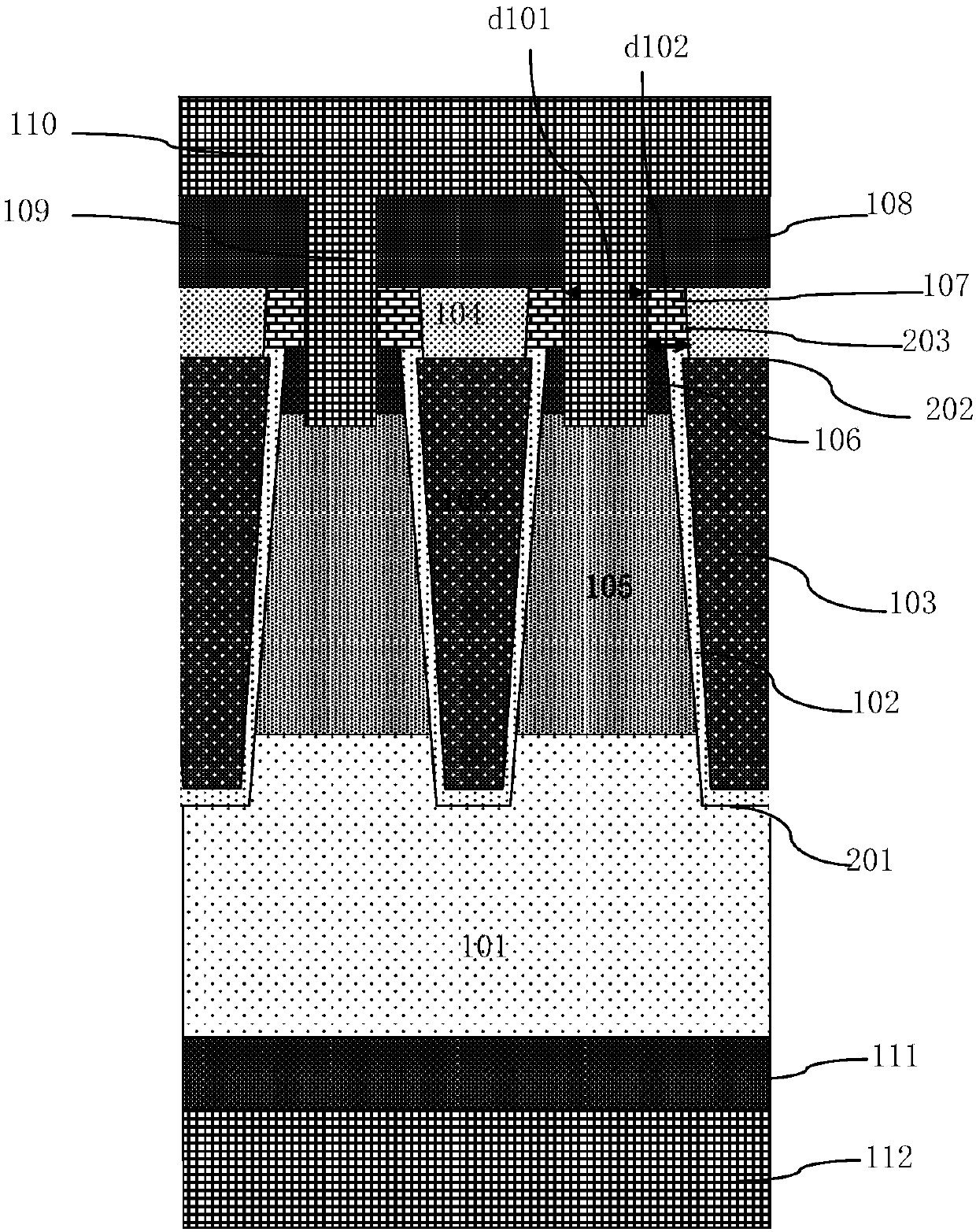
[0081] In order to illustrate the device of the first embodiment of the present invention more clearly, the device of the first embodiment of the present invention is further described in conjunction with specific parameters:

[0082] For a 20V trench gate MOSFET device, a highly doped phosphorus semiconductor substrate 101 is usually used, the resistivity of the semiconductor substrate 101 is 0.0011Ω*cm, and the thickest thickness of the semiconductor substrate 101 after thinning is 150 μm. Usually, a semiconductor epitaxial layer, such as a silicon epitaxial layer, is further formed on the surface of the semiconductor substrate 101 , and the trench gate is formed in the semiconductor epitaxial layer. The semiconductor epitaxial layer is a single-layer epitaxial layer, the resistivity of the epitaxial layer is 0.15Ω*cm, and the thickness of the epitaxial layer is 4 μm. The gate trench 201 of the trench gate MOSFET device has a width of 0.2 μm.

[0083] The opening of the ga...

no. 2 example

[0093] Trench gate MOSFET device of the second embodiment of the present invention:

[0094] The difference between the device of the first embodiment of the present invention is that the trench gate MOSFET device of the second embodiment of the present invention has the following features:

[0095] The trench gate MOSFET also has a shielding layer, which is an SGT MOSFET, and the shielding layer is formed in the gate trench 201 at the bottom of the gate conductive material layer 103, and the material of the shielding layer is conductive to the gate. The materials of the material layer 103 are the same, a shielding medium layer is isolated between the shielding layer and the bottom surface and side surfaces of the gate trench 201, and a gate gap is separated between the shielding layer and the gate conductive material layer 103. Isolated dielectric layer.

[0096] In fact, for SGT MOSFETs, reducing the width of Mesa is more meaningful. This is because for SGT, the shielding ...


PUM

PropertyMeasurementUnit
electrical resistivityaaaaaaaaaa
thicknessaaaaaaaaaa
electrical resistivityaaaaaaaaaa

Abstract

The invention discloses a trench gate MOSFET device. According to the device, a trench gate comprises a gate trench, a gate dielectric layer and a gate conductive material layer; the gate trench is formed in a semiconductor substrate; the gate conductive material layer is filled in the gate trench; a first self-alignment back-etching groove formed by self-alignment back-etching of the gate conductive material layer is formed in the top of the gate groove; the first self-aligning back-etching groove is filled with a first dielectric layer; a second self-aligning back-etching groove formed by taking the first dielectric layer as a self-aligning condition to carry out back-etching on a semiconductor material is formed in a semiconductor platform area between the gate trenches; a channel region and a source region are formed at the bottom of the second self-aligning back-etching groove, and a side wall is formed on the side surface of the second self-aligning back-etching groove; and a source contact hole is self-aligned and defined by the side wall. The invention further discloses a manufacturing method of the trench gate MOSFET device. According to the invention, the contact hole atthe top of the source region can be self-aligned and defined, so that the stepping of the device can be reduced so as to reduce the specific on-resistance of the device.

Description

technical field [0001] The invention relates to the field of manufacturing semiconductor integrated circuits, in particular to a trench gate MOSFET device; the invention also relates to a manufacturing method of the trench gate MOSFET device. Background technique [0002] Such as figure 1 As shown, it is a schematic structural diagram of an existing trench gate MOSFET device, including: a highly doped semiconductor substrate such as a silicon substrate 1, and the resistivity of the silicon substrate 1 is usually between 0.001Ω*cm and 0.002Ω*cm , the thickness of the silicon substrate 1 is also desired to be as thin as possible to reduce the substrate resistance. [0003] An epitaxial layer such as a silicon epitaxial layer 2 is formed on the surface of the silicon substrate 1 , and the thickness and doping concentration of the silicon epitaxial layer 2 determine the device voltage of the device. The higher the breakdown voltage of the device, the thicker the silicon epitax...

Claims


Application Information

Patent Timeline
Patent Type & Authority Applications(China)
IPC IPC(8): H01L29/78H01L21/336
CPCH01L29/7813H01L29/66734
Inventor 蒋容
Owner SHENZHEN SANRISE TECH CO LTD
Why Eureka
Try Eureka