

A white light organic light emitting diode including thermally activated delayed fluorescent material and preparation method thereof
A technology of thermally activated delay and light-emitting diodes, which is applied in the fields of luminescent materials, chemical instruments and methods, semiconductor/solid-state device manufacturing, etc. It can solve complex device structures with multiple light-emitting layers, stricter production process requirements, and hinder commercialization processes, etc. Problems, achieve high color rendering index, reduce processing costs, and reduce material costs
- Summary
- Abstract
- Description
- Claims
- Application Information
AI Technical Summary
Problems solved by technology
Method used
Image

Examples
Embodiment 1
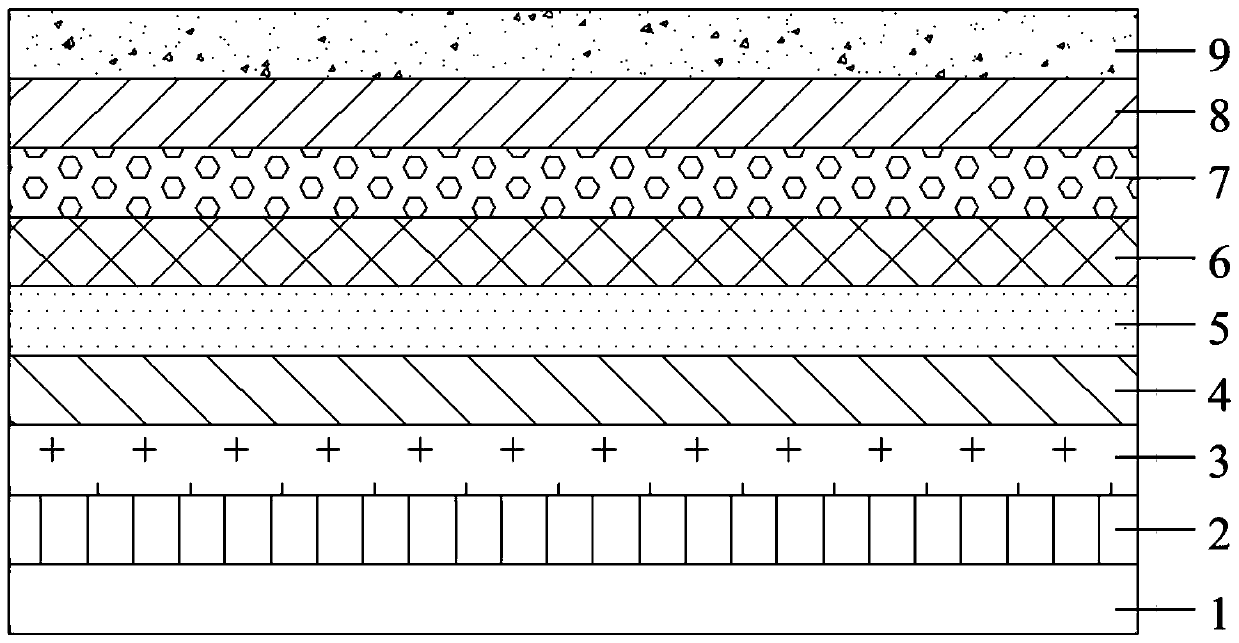
[0053] A white light organic light emitting diode comprising a thermally activated delayed fluorescence material, such as figure 1 As shown, it includes a substrate 1, an anode 2 formed on the surface of the substrate, a hole injection layer 3 formed on the surface of the anode, a hole transport layer 4 formed on the surface of the hole injection layer, and a hole transport layer 4 formed on the surface of the hole transport layer. The electron-exciton blocking layer 5, the light-emitting layer 6 formed on the surface of the electron-exciton blocking layer, the electron transport layer 7 formed on the surface of the light-emitting layer, the electron injection layer 8 formed on the surface of the electron transport layer, and the electron injection layer formed on the surface of the electron injection layer surface of the cathode 9 .
[0054] The preparation method is as follows:
[0055] 1) Clean the etched ITO conductive glass substrate sequentially with a cleaning agent, u...
Embodiment 2
[0070] A white light organic light-emitting diode comprising a thermally activated delayed fluorescent material, the structure of which is the same as in Example 1, and the preparation method is as follows:
[0071] 1) The cleaning process of the ITO glass substrate is the same as in Example 1, and it is directly transferred to the vacuum evaporation chamber after oxygen plasma treatment.
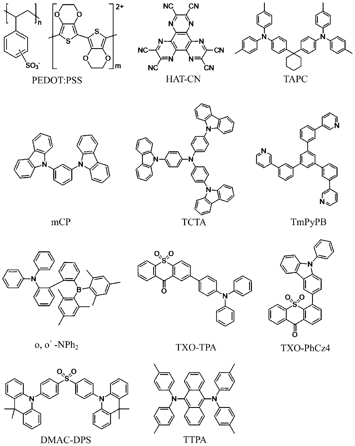
[0072]2) After the vacuum reaches the required value, the hole injection layer material HAT-CN, the hole transport layer material TAPC, the electron-exciton blocking layer material mCP, the light emitting layer material TXO-PhCz4 and o,o'-NPh2 are sequentially evaporated The blend film (mass ratio is TXO-PhCz4:o,o'-NPh 2 =1:100), electron transport layer material TmPyPB, electron injection layer material LiF, cathode material metal Al.
[0073] The evaporation rate and thickness of each functional layer are monitored in real time by a film thickness monitor, and the respective control rate...
PUM
| Property | Measurement | Unit |
|---|---|---|
| thickness | aaaaa | aaaaa |
| quantum efficiency | aaaaa | aaaaa |
| external quantum efficiency | aaaaa | aaaaa |
Abstract
Description
Claims
Application Information