Switching MOS bootstrap charging circuit for gate drive of high speed gan power devices

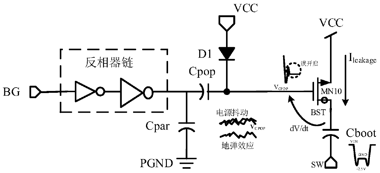
A power device and charging circuit technology, which is applied in the field of switching MOS bootstrap charging circuit driven by the gate of high-speed GaN power devices, can solve the problem of wrong opening of switch tube MN10, unstable gate voltage of switch tube MN10, and overcharging of bootstrap capacitor Cboot. and other problems to achieve the effect of preventing overcharging and overcoming difficult integration.

Active Publication Date: 2019-12-27
UNIV OF ELECTRONICS SCI & TECH OF CHINA
View PDF3 Cites 0 Cited by
  • Summary
  • Abstract
  • Description
  • Claims
  • Application Information

AI Technical Summary

Problems solved by technology

[0011] Aiming at the problems of unstable gate voltage of the switching tube MN10 and overcharging of the bootstrap capacitor Cboot existing in the above-mentioned traditional switching MOS bootstrap circuit, the present invention proposes a switching MOS bootstrap charging circuit, which can be applied to high-speed GaN power devices. The gate drive circuit is used to solve the problems of wrong turn-on of the switch tube MN10 and overcharging of the bootstrap capacitor Cboot

Method used


Image

  • Switching MOS bootstrap charging circuit for gate drive of high speed gan power devices
  • Switching MOS bootstrap charging circuit for gate drive of high speed gan power devices
  • Switching MOS bootstrap charging circuit for gate drive of high speed gan power devices

Examples


Embodiment Construction

[0042] The present invention will be described in detail below in conjunction with the accompanying drawings and specific embodiments.

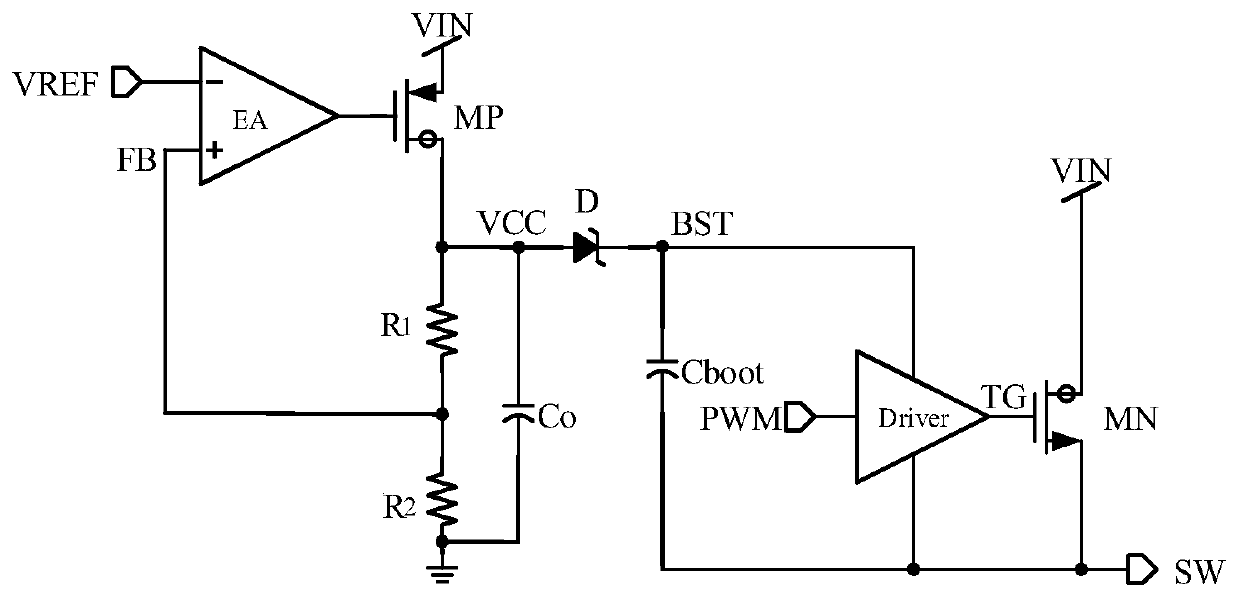
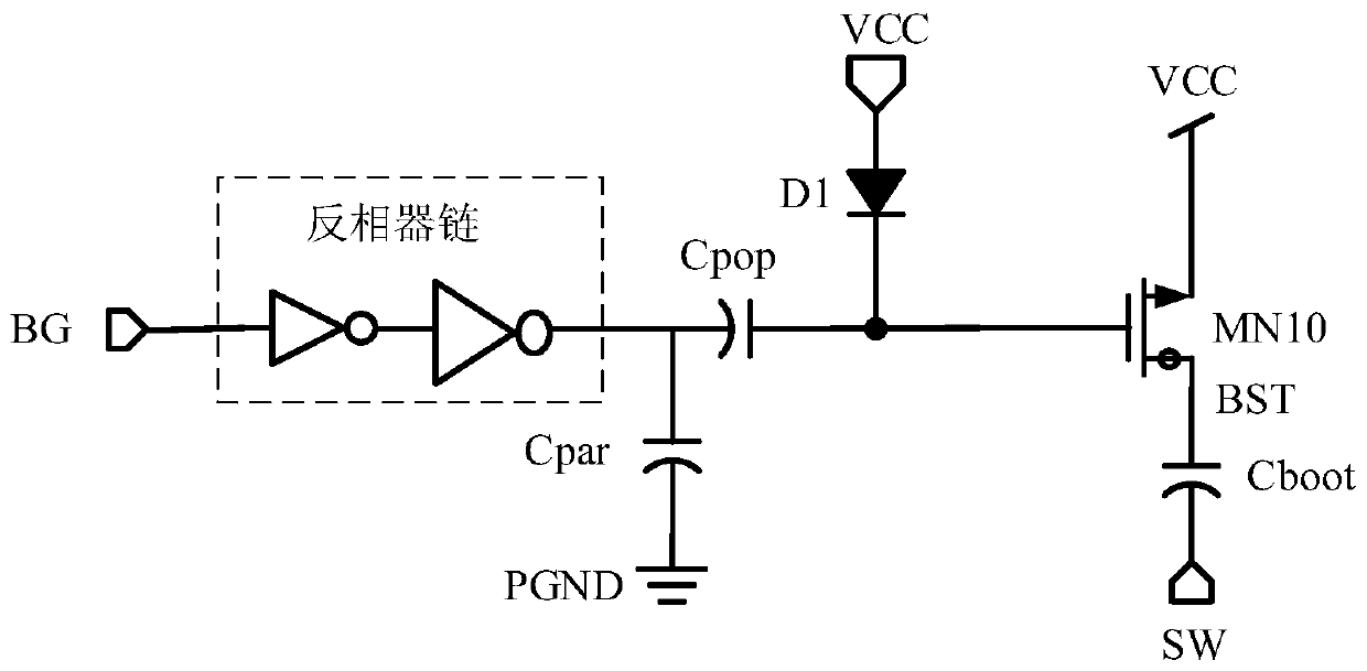
[0043] The switching MOS bootstrap charging circuit proposed by the present invention includes an inverter chain, a diode D1, a charge pump capacitor Cpop, and a switch tube MN10. The output end of the inverter chain is connected to the cathode of the diode D1 after the charge pump capacitor Cpop, and the diode D1 The anode of the switching tube MN10 is connected to the power supply voltage VCC; the gate of the switch tube MN10 is connected to the cathode of the diode D1, and its drain is used as the output terminal of the switching MOS bootstrap charging circuit; the switching MOS bootstrap charging circuit also includes a level shift module and a constant current source module And the switch module, the input terminal of the level shift module is used as the input terminal of the switch MOS bootstrap charging circuit, and its output terminal...


PUM


Abstract

The invention relates to a switching MOS bootstrap charging circuit suitable for gate driving of high-speed GaN power devices, and belongs to the technical field of electronic circuits. It includes an inverter chain, a diode, a charge pump capacitor, and a switch tube. The output terminal of the inverter chain is connected to the cathode of the diode after passing through the charge pump capacitor, and the anode of the diode is connected to the power supply voltage; the gate of the switch tube is connected to the cathode of the diode, and its The drain is used as the output terminal of the switch MOS bootstrap charging circuit; the switch MOS bootstrap charging circuit also includes a level shift module, a constant current source module and a switch module, and the input terminal of the level shift module is used as the input of the switch MOS bootstrap charging circuit terminal, the output terminal of which is connected to the input terminal of the inverter chain; the constant current source module is connected between the grid of the switching tube and the ground; the switching module is connected between the source of the switching tube and the power supply voltage. The invention can solve the problems of wrongly turning on the switching tube and overcharging of the bootstrap capacitor existing in the traditional switch MOS bootstrap circuit.

Description

technical field [0001] The invention belongs to the technical field of electronic circuits, and relates to a bootstrap circuit suitable for high-speed driving circuits, in particular to a switching MOS bootstrap charging circuit suitable for gate driving of high-speed GaN power devices. Background technique [0002] In a BUCK converter, a drive circuit is usually required to control the upper and lower power transistors to turn on. During the turn-on process of the lower power transistor, the switch node SW is pulled down to the ground potential VSS; while in the turn-on process of the upper power transistor, the potential at the switch node SW is gradually pulled up to the input level VIN, thus, the potential at the switch node SW is It floats between the input level VIN and the ground potential VSS. In the gate drive circuit where the upper power transistor is NMOS, the source potential of the upper power transistor is the potential at the switch node SW, so the gate of t...

Claims


Application Information

Patent Timeline
Patent Type & Authority Patents(China)
IPC IPC(8): H02M1/08
CPCH02M1/08Y02B70/10
Inventor 明鑫辛杨立胡晓冬张宣潘溯王卓张波
Owner UNIV OF ELECTRONICS SCI & TECH OF CHINA
Why Eureka
Try Eureka