A method for determining relationship parameters of transistors in an array substrate grid drive circuit

A gate drive circuit, array substrate technology, applied in instruments, static indicators, etc., can solve problems such as difficulty in optimizing transistor design parameters, affecting control signal point voltage or voltage waveform, etc., to achieve a simple and efficient simulation method and save layout space , the effect of improving stability

Active Publication Date: 2018-11-16
TCL CHINA STAR OPTOELECTRONICS TECH CO LTD
View PDF3 Cites 0 Cited by
  • Summary
  • Abstract
  • Description
  • Claims
  • Application Information

AI Technical Summary

Problems solved by technology

Each transistor included in the GOA drive unit will affect the voltage or voltage waveform of the control signal point Q(n), making it difficult to optimize the best design parameters of the transistor, which needs to be improved urgently

Method used


Image

  • A method for determining relationship parameters of transistors in an array substrate grid drive circuit
  • A method for determining relationship parameters of transistors in an array substrate grid drive circuit
  • A method for determining relationship parameters of transistors in an array substrate grid drive circuit

Examples


Embodiment Construction

[0028] Reference will now be made in detail to embodiments of the present invention, examples of which are illustrated in the accompanying drawings, wherein like numerals refer to like parts throughout. The embodiments are described below in order to explain the present invention by referring to the figures.

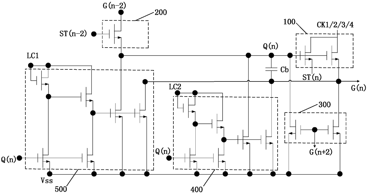
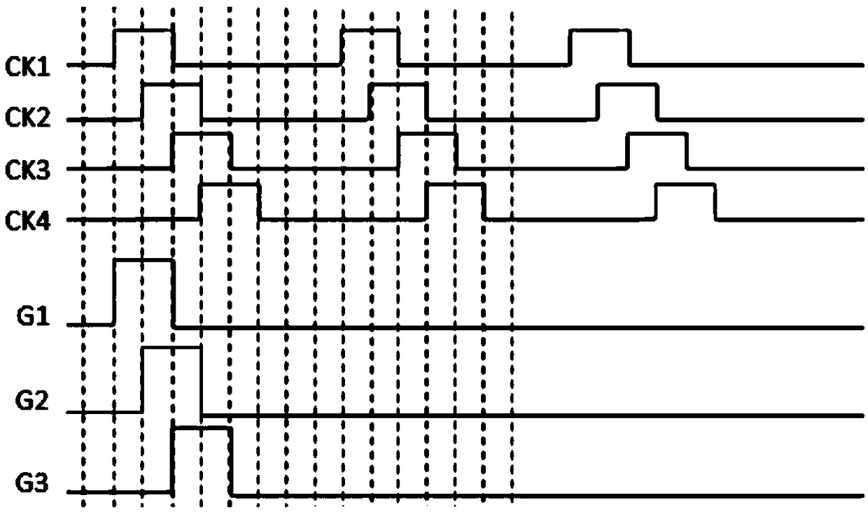
[0029] Refer below Figure 3 to Figure 6 A method for determining relational parameters of transistors in a gate driving circuit of an array substrate according to an embodiment of the present invention is described.

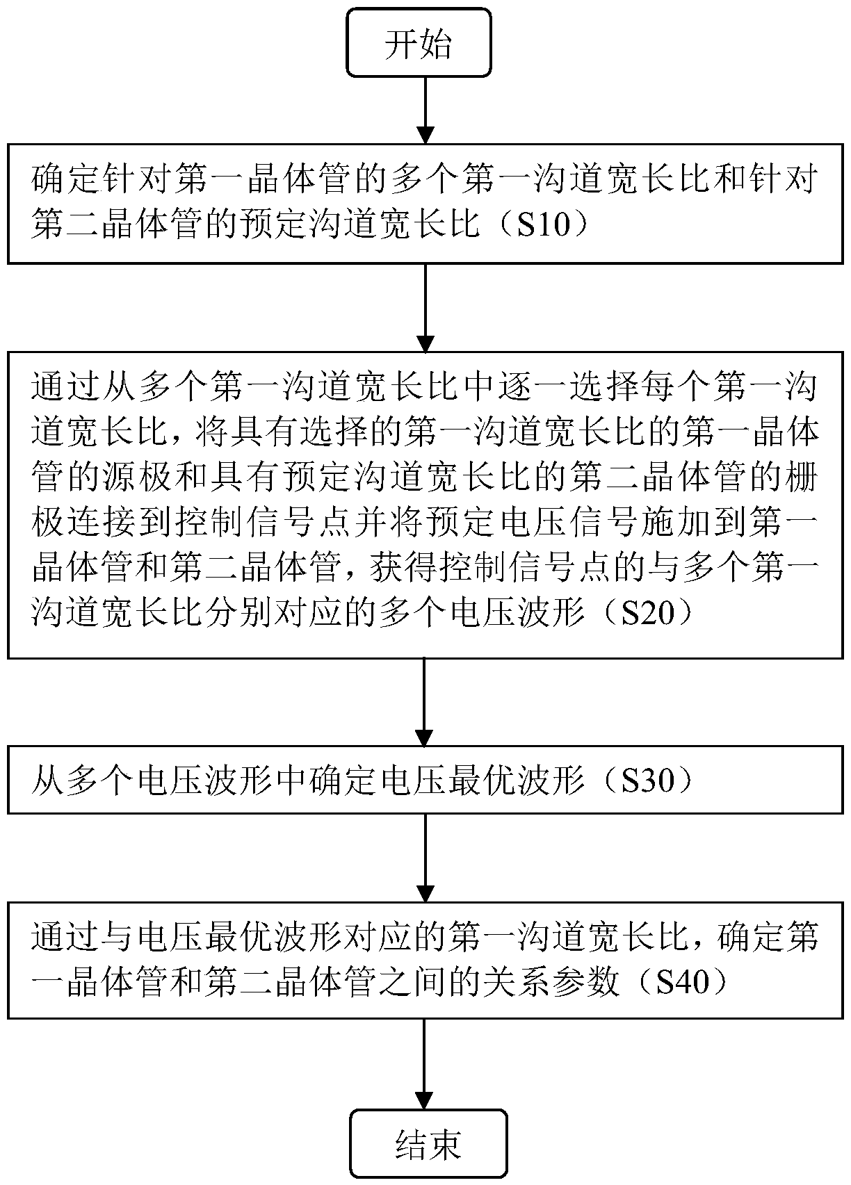
[0030] image 3 A flow chart showing a method for determining relational parameters of transistors in a gate driving circuit of an array substrate according to an exemplary embodiment of the present invention.

[0031] refer to image 3 , in step S10, it is determined that for the first transistor T 1 multiple of the first channel width-to-length ratio and for the second transistor T 2 The predetermined channel width-to-length ratio.

[0032] Here, t...


PUM


Abstract

The invention provides a method for determining relationship parameters of transistors in an array substrate grid drive circuit. The method comprises the following steps: determining a plurality of first channel width-to-length ratios for a first transistor and a preset channel width-to-length ratio for a second transistor; selecting each first channel width-to-length ratio from the plurality of first channel width-to-length ratios one by one, and connecting the source electrode of the first transistor having the selected first channel width-to-length ratio and the grid electrode of the secondtransistor to a control signal point and applying a preset voltage signal to the first transistor and the second transistor to obtain a plurality of voltage waveforms, corresponding to the pluralityof first channel width-to-length ratios, of the control signal point; determining an optimal voltage waveform from the plurality of voltage waveforms; and determining the relationship parameters between the first transistor and the second transistor according to the first channel width-to-length ratio corresponding to the optimal voltage waveform. The method can greatly improve transistor performance stability, save layout space and facilitate design of a narrow frame of a panel.

Description

technical field [0001] The present invention relates to the technical field of displays, and more specifically, to a method for determining relational parameters of transistors in a gate drive circuit of an array substrate. Background technique [0002] Array substrate gate drive (Gate Driver OnArray, GOA) technology is a kind of thin film transistor (ThinFilm Transistor, TFT) gate scanning drive circuit fabricated on the array substrate to replace the drive chip made of external silicon chips technology. The gate voltage of each row of TFTs in the liquid crystal display can be provided by the GOA circuit. [0003] Existing array substrate gate driving circuits usually include a plurality of cascaded GOA driving units, and each level of GOA driving units corresponds to driving one level of horizontal scanning lines. figure 1 A block diagram showing a GOA drive unit in an existing array substrate gate drive circuit, figure 2 show figure 1 timing diagram. Such as figure...

Claims


Application Information

Patent Timeline
Patent Type & Authority Applications(China)
IPC IPC(8): G09G3/36
CPCG09G3/3674
Inventor 宋乔乔
Owner TCL CHINA STAR OPTOELECTRONICS TECH CO LTD
Why Eureka
Try Eureka