Array substrate, dispLay paneL and dispLay device
A technology for array substrates and display panels, applied in nonlinear optics, instruments, optics, etc., can solve problems affecting product quality, etc., and achieve the effect of improving flattening effect, improving product quality, and uniform film thickness
- Summary
- Abstract
- Description
- Claims
- Application Information
AI Technical Summary
Problems solved by technology
Method used
Image

Examples
Embodiment 1
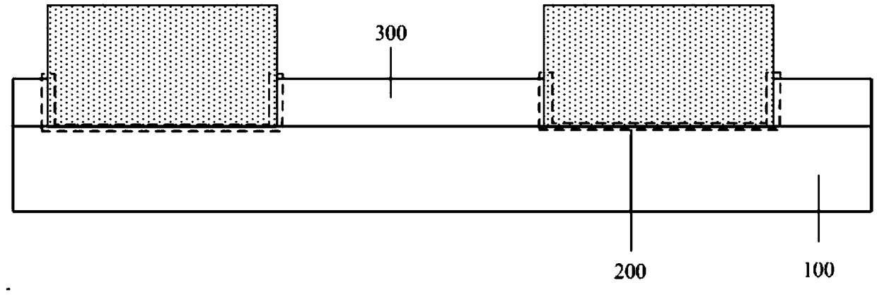
[0032] In specific implementation, in the embodiment of the present invention, such as image 3 As shown, the array substrate may include: a target film layer 300 located between the base substrate 100 and the color resist layer 112 . Wherein, the target film layer 300 has a recessed structure 200; the recessed structure 200 penetrates the target film layer 300, that is, the recessed structure 200 may be a via hole. In this way, a recessed structure penetrating through the target film layer is provided in the target film layer to fill the recessed structure with the color resist layer, thereby reducing the level difference between the color resist layer and the source-drain layer.
[0033] Generally, for the array substrate, there are generally multiple film layers of one whole layer disposed thereon. The recessed structure provided on the array substrate can be formed by simultaneously removing multiple film layers located in the pixel opening area in the array substrate, or c...
Embodiment 2
[0040] In specific implementation, in the embodiment of the present invention, such as Figure 5 As shown, the array substrate may include: a target film layer 300 located between the base substrate 100 and the color resist layer 112 . Wherein, the target film layer 300 has a recessed structure 200; the thickness of the target film layer 300 in the area where the recessed structure 200 is located is smaller than the thickness of the target film layer 300 in other areas. In this way, the recessed structure is formed by thinning the target film layer, so as to fill the recessed structure with the color resist layer, thereby reducing the level difference between the color resist layer and the source-drain layer.
[0041] Generally, for the array substrate, there are generally multiple film layers of one whole layer disposed thereon. The concave structure provided on the array substrate can be formed by simultaneously thinning the multi-layer film layers located in the pixel open...
Embodiment 3
[0048] Of course, the base substrate can also be thinned to form a recessed structure. In specific implementation, such as Figure 8 and Figure 9 As shown, the base substrate 100 has a first surface S1 facing the color resist layer 112, and the first surface S1 has a recessed structure 200; the thickness of the base substrate 100 in the area where the recessed structure 200 is located is smaller than the thickness of the base substrate 100 in other areas . In this way, when the base substrate 100 is thinned to form a concave structure, and then other film layers are sequentially arranged on the base substrate 100, such as the interlayer dielectric layer 140, the gate insulating layer 130, and the buffer layer 160, due to the formation of the same film layer The thicknesses are generally the same, and finally a recessed structure can be formed in the opening area of the pixel unit, so that the color resist layer can be directly filled in the recessed structure, thereby red...
PUM
 Abstract
Description
Claims
Application Information
 - R&D
- Intellectual Property
- Life Sciences
- Materials
- Tech Scout
- Unparalleled Data Quality
- Higher Quality Content
- 60% Fewer Hallucinations
Browse by: Latest US Patents, China's latest patents, Technical Efficacy Thesaurus, Application Domain, Technology Topic, Popular Technical Reports.
© 2025 PatSnap. All rights reserved.Legal|Privacy policy|Modern Slavery Act Transparency Statement|Sitemap|About US| Contact US: help@patsnap.com