Image display method and device based on pixel compensation, display device and medium

A technology of image display and display equipment, applied in the field of image processing, can solve problems such as complex circuit structure, affecting OLED light-emitting area, difficult integration, etc., to achieve the effect of improving display effect and avoiding uneven brightness display

Inactive Publication Date: 2018-11-23
SHENZHEN SKYWORTH RGB ELECTRONICS CO LTD
View PDF9 Cites 21 Cited by
  • Summary
  • Abstract
  • Description
  • Claims
  • Application Information

AI Technical Summary

Problems solved by technology

However, the above-mentioned circuit structure is relatively complex, and the response speed is slow, the compensation range is small, the cost is high, and it is difficult to integrate on the substrate, which affects the light-emitting area of ​​the OLED.

Method used


Image

  • Image display method and device based on pixel compensation, display device and medium
  • Image display method and device based on pixel compensation, display device and medium
  • Image display method and device based on pixel compensation, display device and medium

Examples


Embodiment 1

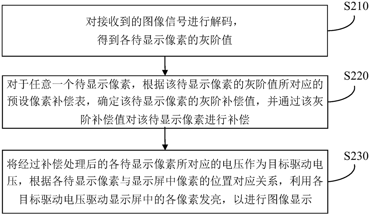
[0053] figure 2 It is a flow chart of an image display method based on pixel compensation provided in Embodiment 1 of the present invention. The method can be executed by an image display device based on pixel compensation, and the device can be implemented by software and / or hardware. Typical It can be integrated in display devices such as televisions. see figure 2 , the method of this embodiment specifically includes:

[0054] S210. Decode the received image signal to obtain the gray scale value of each pixel to be displayed.

[0055] First of all, it needs to be explained that when the display screen is displaying images, it is necessary to control the thin-film transistor (Thin-Film Transistor, TFT) of each pixel unit in the display screen to turn on through the driving voltage, so that the thin-film transistor generates a driving current, so that each pixel unit in the display screen Lights up for image display. Since the number of TFTs corresponds to the number of ...

Embodiment 2

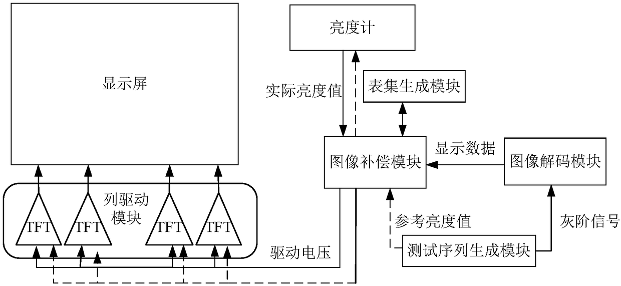
[0071] Figure 4 A structural block diagram of a pixel compensation device for a display device provided in Embodiment 2 of the present invention, as shown in Figure 4 As shown, the device includes: an image decoding module 310 , an image compensation module 320 and an image display module 330 .

[0072] Wherein, the image decoding module 310 is configured to decode the image signal received by the display device to obtain the gray scale value of each pixel to be displayed;

[0073] The image compensation module 320 is configured to, for any pixel to be displayed, determine the gray scale compensation value of the pixel to be displayed according to the preset pixel compensation table corresponding to the gray scale value of the pixel to be displayed, and use the gray scale compensation value to Compensating the pixel to be displayed;

[0074] The image display module 330 is configured to use the voltage corresponding to each pixel to be displayed after compensation processi...

Embodiment 3

[0091] Figure 5 It is a schematic structural diagram of a display device provided by Embodiment 3 of the present invention. Figure 5 A block diagram of an exemplary display device 12 suitable for use in implementing embodiments of the invention is shown. Figure 5 The displayed display device 12 is only an example, and should not limit the functions and scope of use of the embodiments of the present invention.

[0092] Such as Figure 5 As shown, display device 12 takes the form of a general purpose computing device. Components of display device 12 may include, but are not limited to: one or more processors or processing units 16 , system memory 28 , bus 18 connecting various system components including system memory 28 and processing unit 16 .

[0093] Bus 18 represents one or more of several types of bus structures, including a memory bus or memory controller, a peripheral bus, an accelerated graphics port, a processor, or a local bus using any of a variety of bus struc...


PUM


Abstract

The embodiment of the invention discloses an image display method and device based on pixel compensation, a display device and a medium. The method comprises the steps of decoding received image signals to obtain the gray scale value of each pixel to be displayed; for any pixel to be displayed, determining the gray scale compensation value of the pixel to be displayed according to a preset pixel compensation table corresponding to the gray scale value of the pixel to be displayed, compensating the pixel to be displayed through the gray scale compensation value; and driving the each pixel unitin a display screen to shine by using each target driving voltage so as to display images, by taking the voltage corresponding to each pixel to be displayed after compensation processing as target driving voltage based on the correspondence relation of the pixels to be displayed and the positions of the pixel units in the display screen. By the adoption of the technical scheme, the influence of uneven display brightness of pixels in the display screen on image display is effectively avoided, and the image display quality is greatly improved.

Description

technical field [0001] The embodiments of the present invention relate to the technical field of image processing, and in particular to an image display method, device, display device and medium based on pixel compensation. Background technique [0002] Active-matrix organic light-emitting diode panel (active-matrix organic light-emitting diode, AMOLED) referred to as OLED in the present invention has the advantages of low power consumption, self-illumination, good image quality and fast response speed, and is currently developing rapidly and application. Low Temperature Poly-Silicon Thin-Film Transistor (LTPS TFT) and Oxide Thin-Film Transistor (Oxide TFT) have higher mobility and more stable characteristics, and are widely used in display devices with OLED displays. Used to control the driving current of the OLED. [0003] At present, no matter whether LTPS TFT or Oxide TFT is used, the electrical parameters such as the threshold voltage and mobility of the TFT correspon...

Claims


Application Information

Patent Timeline
Patent Type & Authority Applications(China)
IPC IPC(8): G09G3/3233
CPCG09G3/3233
Inventor 徐遥令李坚王俊生
Owner SHENZHEN SKYWORTH RGB ELECTRONICS CO LTD
Why Eureka
Try Eureka