
Dynamic random access memory and method of making the same

A technology of dynamic random access and manufacturing method, which is applied in the direction of semiconductor devices, electric solid-state devices, electrical components, etc., can solve the problems of reducing the reliability of dynamic random access memory, short circuit, and increase of contact resistance, so as to improve the sensing margin degree, increase the contact area, and reduce the effect of capacitance value

Active Publication Date: 2021-01-26
WINBOND ELECTRONICS CORP
View PDF3 Cites 1 Cited by
  • Summary
  • Abstract
  • Description
  • Claims
  • Application Information

AI Technical Summary

Problems solved by technology

That is to say, the critical dimension in the DRAM is gradually reduced, which causes the contact resistance between the capacitor contact window and the storage capacitor in the DRAM to increase, thereby reducing the reliability of the DRAM. (reliability)
Once the misalignment of the bit line occurs, the short circuit between the bit line and the capacitor contact window will become worse

Method used


Image

  • Dynamic random access memory and method of making the same
  • Dynamic random access memory and method of making the same
  • Dynamic random access memory and method of making the same

Examples


Embodiment Construction

[0051] The present invention will be described more fully with reference to the accompanying drawings of this embodiment. However, the present invention can also be embodied in various forms and should not be limited to the embodiments described herein. In the drawings, the thicknesses of layers and regions may be exaggerated for clarity. The same or similar reference numerals denote the same or similar elements, and the following paragraphs will not repeat them one by one.

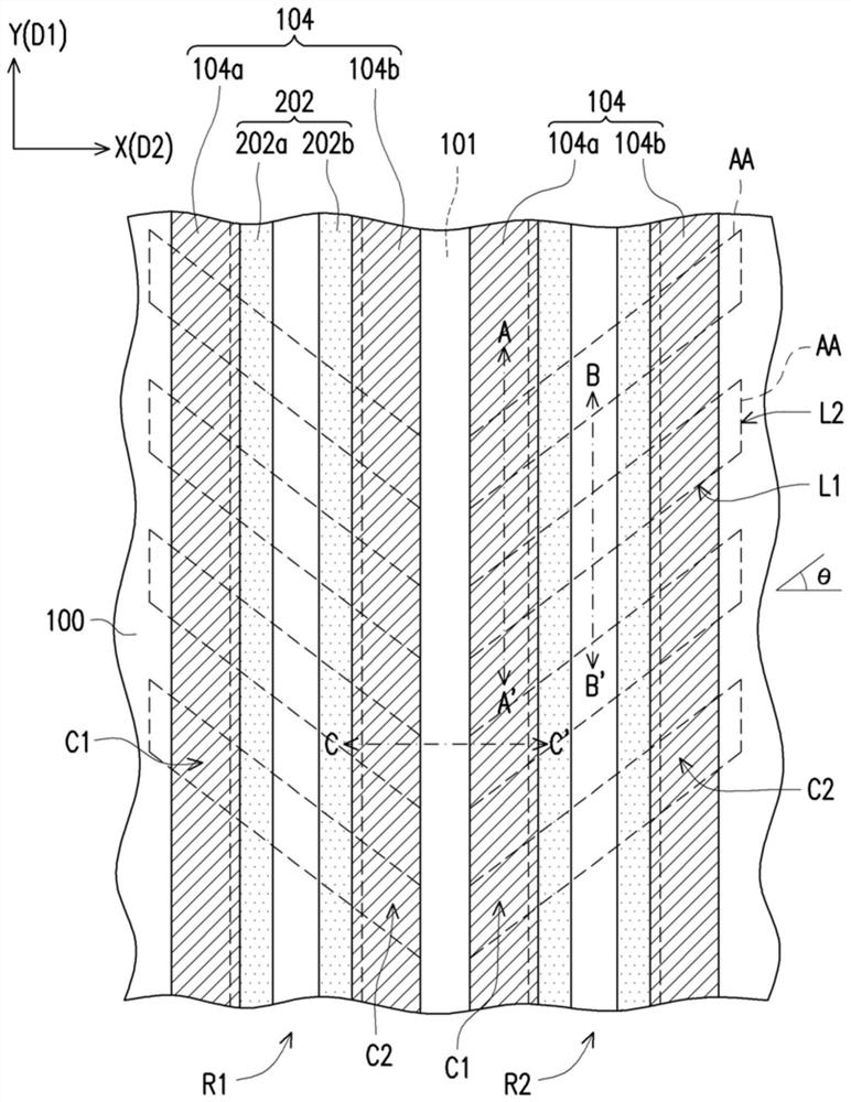
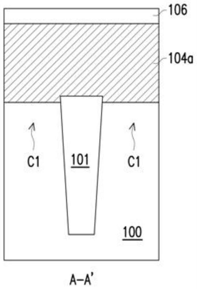
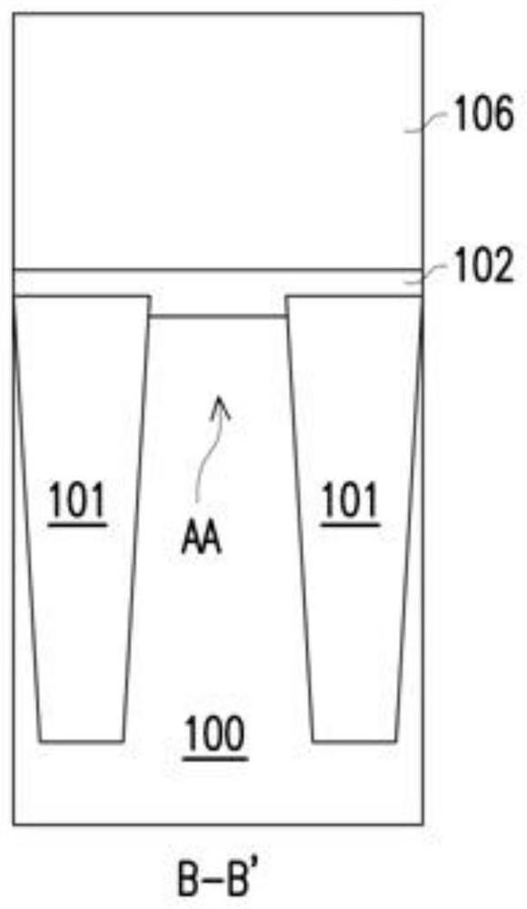
[0052] Figure 2A to Figure 2D , Figure 3A to Figure 3D , Figure 4A to Figure 4D The stages of the fabrication process for a single memory cell structure are shown.

[0053] Please refer to Figure 1A , Figure 2A , Figure 3A , Figure 4A , the first embodiment provides a DRAM manufacturing method, the steps are as follows. First, a substrate 100 is provided, and the substrate 100 has a plurality of active regions AA. The active areas AA are configured in strips and arranged in an array. In ...


PUM


Abstract

The invention provides a dynamic random access memory and its manufacturing method. The memory includes a base, a plurality of isolation structures, a plurality of conductor structure groups, a plurality of bit line structures and a plurality of spacers. The substrate has multiple active regions. The isolation structure is located in the base and extends along the first direction. Each isolation structure is disposed between two adjacent active regions. The conductor structure group is parallelly arranged on the base along the first direction. The bit line structure is parallelly arranged on the substrate along the second direction. The bit line structure runs through the set of conductor structures. The spacer is arranged parallel to the sidewall of the bit line structure along the second direction to electrically isolate the bit line structure and the conductor structure group.

Description

technical field [0001] The invention relates to a memory and a manufacturing method thereof, in particular to a dynamic random access memory and a manufacturing method thereof. Background technique [0002] As technology advances with each passing day, advances in electronic components have increased the need for greater storage capacity. To increase storage capacity, storage elements, especially dynamic random access memories (DRAMs), have become smaller and more densely packed. Therefore, how to integrate more memory cells on one chip is being studied in recent years. [0003] However, as the density of the DRAM increases, it is easy to form a tapered profile when forming a bit line with a high aspect ratio. A bitline having a tapered profile reduces the size of the capacitor contact and increases the possibility of a short circuit between the bitline and the capacitor contact. That is to say, the critical dimension in the DRAM is gradually reduced, which causes the con...

Claims


Application Information

Patent Timeline
Patent Type & Authority Patents(China)
IPC IPC(8): H01L27/1159
CPCH10B51/30H01L29/0649H10B12/315H10B12/0335H10B12/482H10B12/485
Inventor 竹迫寿晃田中义典
Owner WINBOND ELECTRONICS CORP
Learn More