

Substrate, preparation method of substrate and display device
A substrate, substrate substrate technology, applied in semiconductor/solid-state device manufacturing, electrical components, electrical solid-state devices, etc., can solve problems such as uneven thickness of the light-emitting functional layer
- Summary
- Abstract
- Description
- Claims
- Application Information
AI Technical Summary
Problems solved by technology
Method used
Image


Examples
Embodiment Construction
[0029] The following will clearly and completely describe the technical solutions in the embodiments of the present invention with reference to the accompanying drawings in the embodiments of the present invention. Obviously, the described embodiments are only some, not all, embodiments of the present invention. Based on the embodiments of the present invention, all other embodiments obtained by persons of ordinary skill in the art without making creative efforts belong to the protection scope of the present invention.
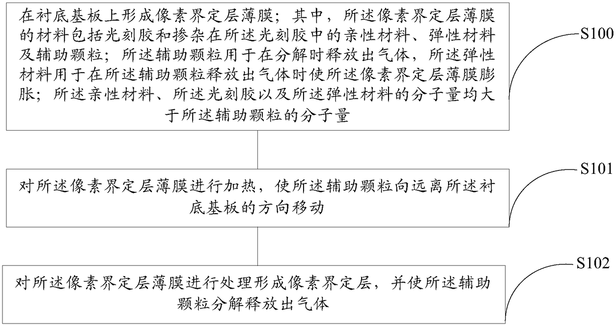
[0030] Embodiments of the present invention provide a method for preparing a substrate, such as figure 2 shown, including:
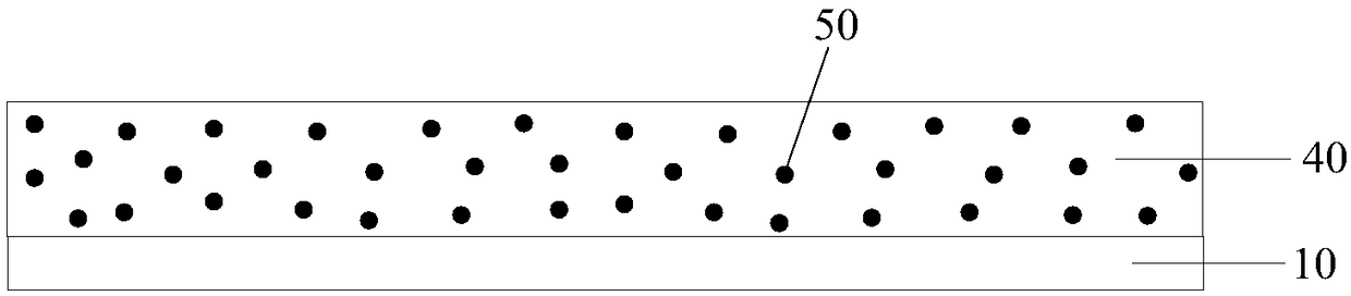
[0031] S100, such as image 3 As shown, a pixel defining layer film 40 is formed on the base substrate 10; wherein, the material of the pixel defining layer film 40 includes photoresist and an affinity material doped in the photoresist, an elastic material and auxiliary particles 50; The particles 50 are used to release gas when decom...
PUM
 Abstract
Description
Claims
Application Information