Micro-LED display panel and manufacturing method thereof

A technology for a display panel and a manufacturing method, which is applied in the manufacture of semiconductor/solid-state devices, electrical components, and electrical solid-state devices, etc., can solve the problems of difficult growth, difficulty in color display of Micro-LED display panels, and high sapphire lattice mismatch rate. , to achieve the more difficult effect

Inactive Publication Date: 2018-11-27
SOUTH UNIVERSITY OF SCIENCE AND TECHNOLOGY OF CHINA
View PDF7 Cites 7 Cited by
  • Summary
  • Abstract
  • Description
  • Claims
  • Application Information

AI Technical Summary

Problems solved by technology

However, due to the small lattice of red and green LED light-emitting crystals, the high lattice mismatch rate with sapphire, the growth is difficult, and the quality of finished products is poor. Therefore, it is difficult to realize the color display of Micro-LED display panels.

Method used


Image

  • Micro-LED display panel and manufacturing method thereof
  • Micro-LED display panel and manufacturing method thereof
  • Micro-LED display panel and manufacturing method thereof

Examples


Embodiment Construction

[0045] In order to make the purpose, technical solutions and advantages of the present invention clearer, the technical solutions of the present invention will be clearly and completely described through implementation with reference to the accompanying drawings in the embodiments of the present invention. Obviously, the described embodiments are the embodiment of the present invention. Some, but not all, embodiments. Based on the embodiments of the present invention, all other embodiments obtained by persons of ordinary skill in the art without making creative efforts belong to the protection scope of the present invention.

[0046] It should be noted that, in the drawings, the same reference numerals represent the same structures or steps.

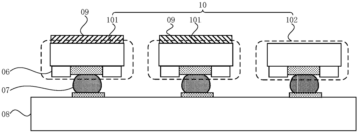
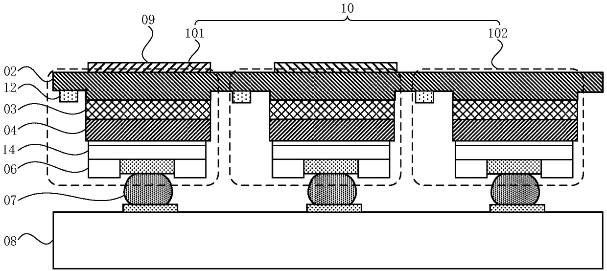
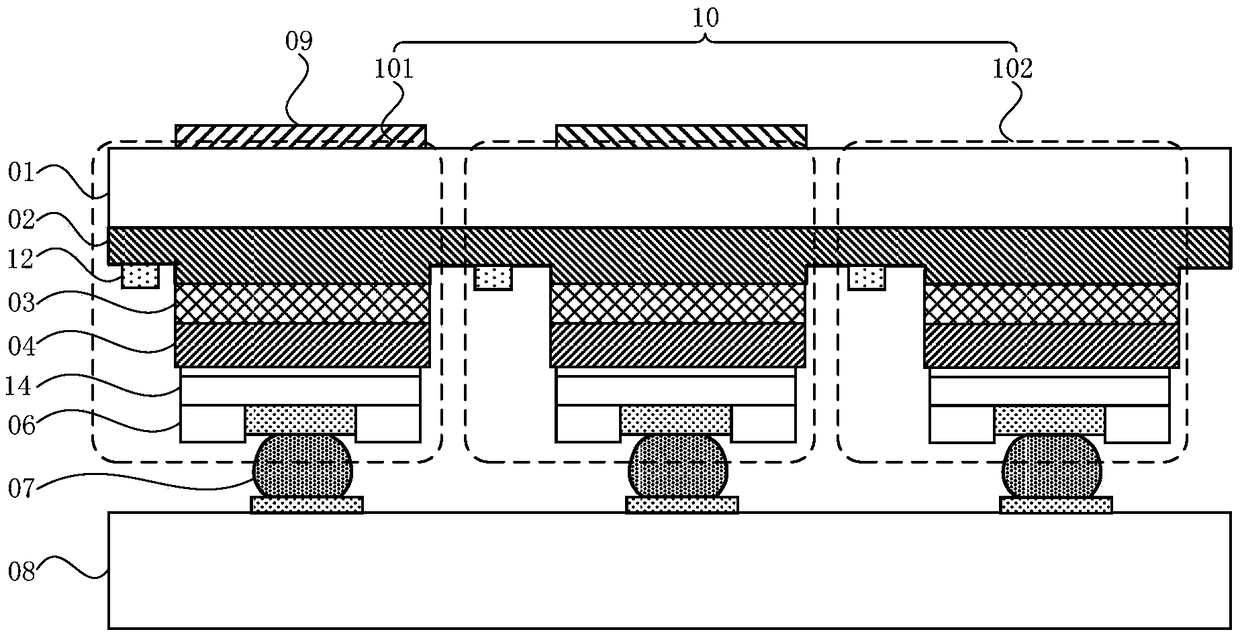
[0047] figure 1 It is a schematic structural diagram of a Micro-LED display panel provided by an embodiment of the present invention. refer to figure 1 , the Micro-LED display panel includes: a bonding substrate 08; an electroluminesc...


PUM


Abstract

The embodiment of the invention discloses a micro-LED display panel and a manufacturing method thereof. The Micro-LED display panel comprises a bonded substrate, an electroluminescent Micro-LED pixelarray and a luminescent dielectric layer, wherein the electroluminescent Micro-LED pixel array is reversely arranged on one side of the bonded substrate and is electrically connected with the bonded substrate, each electroluminescent Micro-LED pixel in the electroluminescent Micro-LED pixel array comprises a first kind of sub pixel and a second kind of sub pixel, the luminescent dielectric layer is arranged on one side, far from the bonded substrate of the first kind of sub pixel, and the luminescent dielectric layer is prepared from the materials of at least one of a perovskite photoluminescent material and nano fluorescent powder. The Micro-LED display panel disclosed by the embodiment of the invention can emit self color light through the second kind of sub pixel, and the first kind ofsub pixel can stimulate the luminescent dielectric layer to emit corresponding color light through the light emitted by the electroluminescence; thus, full-color display of the Micro-LED display panelcan be achieved through mutual match among different luminescent colors, and the problem that color display of the Micro-LED display panel is difficult to achieve in the prior art is solved.

Description

technical field [0001] Embodiments of the present invention relate to display technologies, and in particular to a Micro-LED display panel and a manufacturing method thereof. Background technique [0002] With the development of display technology, the traditional liquid crystal display (Liquid Crystal Display, LCD) technology is gradually unable to meet the needs of the market in terms of color rendering, luminous efficiency, flexibility and portability. The new generation of lighting and display technology has become an investment and research hotspot. A new generation of lighting and display devices includes light emitting diode (Light Emitting Diode, LED) displays, wherein the light emitting diodes include organic light emitting diodes, quantum dot light emitting diodes, micro light emitting diodes and Micro-LEDs. Among them, the pixel size of Micro-LED is smaller than that of micro-light-emitting diodes, which is suitable for indoor screens and small-sized displays. ...

Claims


Application Information

Patent Timeline
Patent Type & Authority Applications(China)
IPC IPC(8): H01L27/12H01L21/77
CPCH01L27/1214H01L27/1259
Inventor 刘召军孙小卫王立铎王凯魏枫闫思吴
Owner SOUTH UNIVERSITY OF SCIENCE AND TECHNOLOGY OF CHINA
Why Eureka
Try Eureka