FPGA (field programmable gate array) and CPU (central processing unit) SDIO (secure digital input output) communication interface implementation method and device

A technology of communication interface and implementation method, applied in program control device, generation of response errors, program control design, etc., can solve the problems of unguaranteed communication reliability, high personnel requirements, heavy workload, etc., and achieve large selection The effect of space, simple code, and less code modification

Active Publication Date: 2018-11-30
JUNENG SPECIAL COMM EQUIP CO LTD TOEC GRP
View PDF4 Cites 6 Cited by
  • Summary
  • Abstract
  • Description
  • Claims
  • Application Information

AI Technical Summary

Problems solved by technology

The workload is heavy, the requirements for personnel are high, it is difficult to implement, and the reliability of communication cannot be guaranteed

Method used


Image

  • FPGA (field programmable gate array) and CPU (central processing unit) SDIO (secure digital input output) communication interface implementation method and device
  • FPGA (field programmable gate array) and CPU (central processing unit) SDIO (secure digital input output) communication interface implementation method and device
  • FPGA (field programmable gate array) and CPU (central processing unit) SDIO (secure digital input output) communication interface implementation method and device

Examples


Embodiment 1

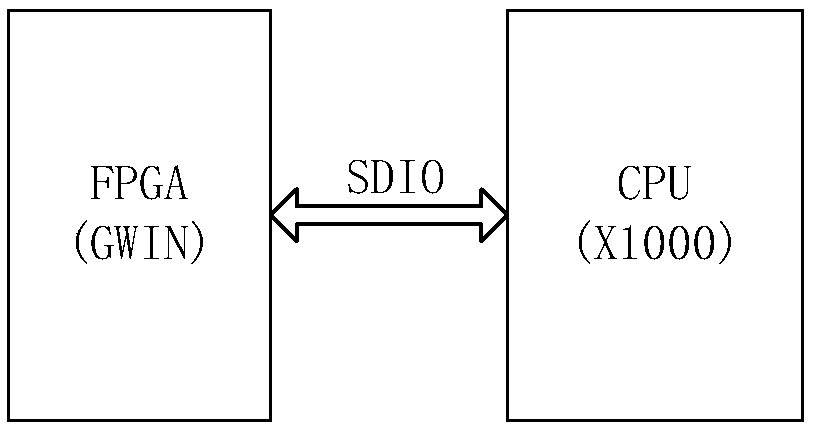
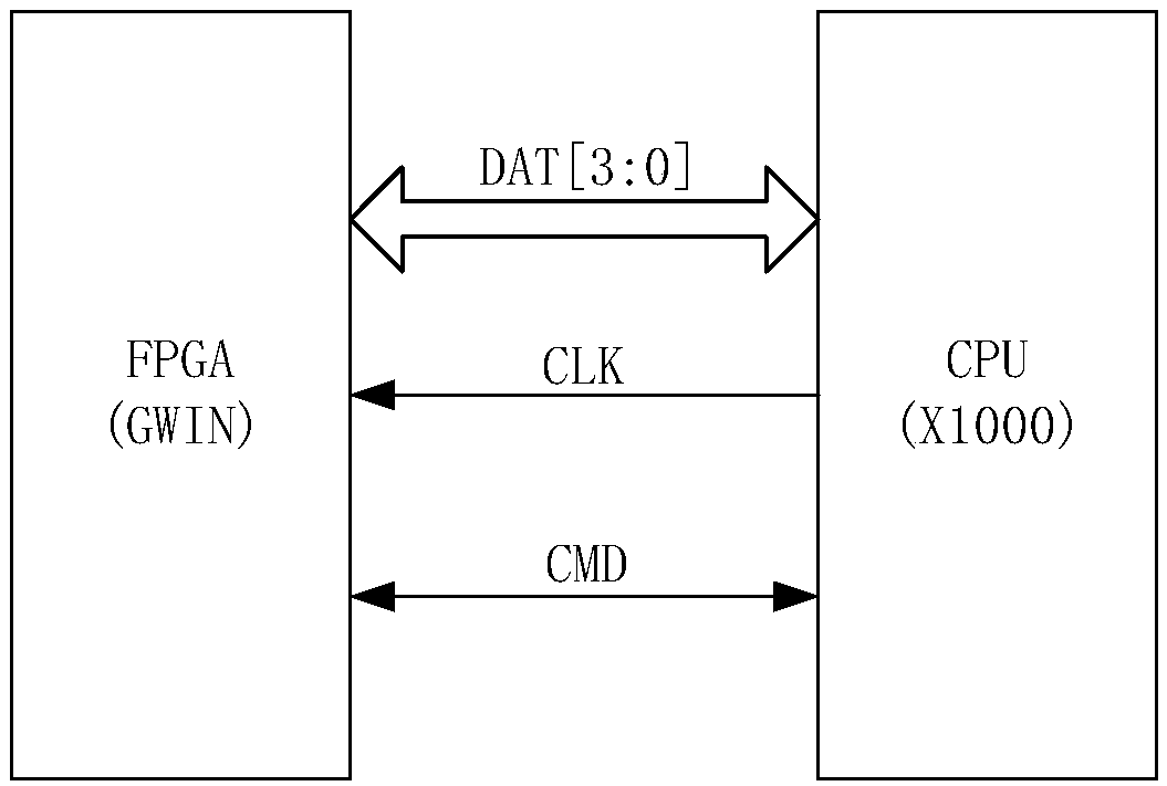
[0114] A method for realizing SDIO communication interface between FPGA and CPU, see Figure 4 , the method includes the following steps:

[0115] 101: The FPGA performs a CRC7 check on the received command packet, and the command can only be responded to if the check is passed;

[0116] 102: The FPGA sends a response, and adds the CRC7 check result at the end of the response packet;

[0117] 103: An SDIO register table is stored inside the FPGA for initialization of SDIO communication;

[0118] 104: The FPGA performs a CRC16 check on the received data, and transmits the check result in the form of an interrupt;

[0119] 105: FPGA transmits data, and adds CRC16 check result at the end of the data.

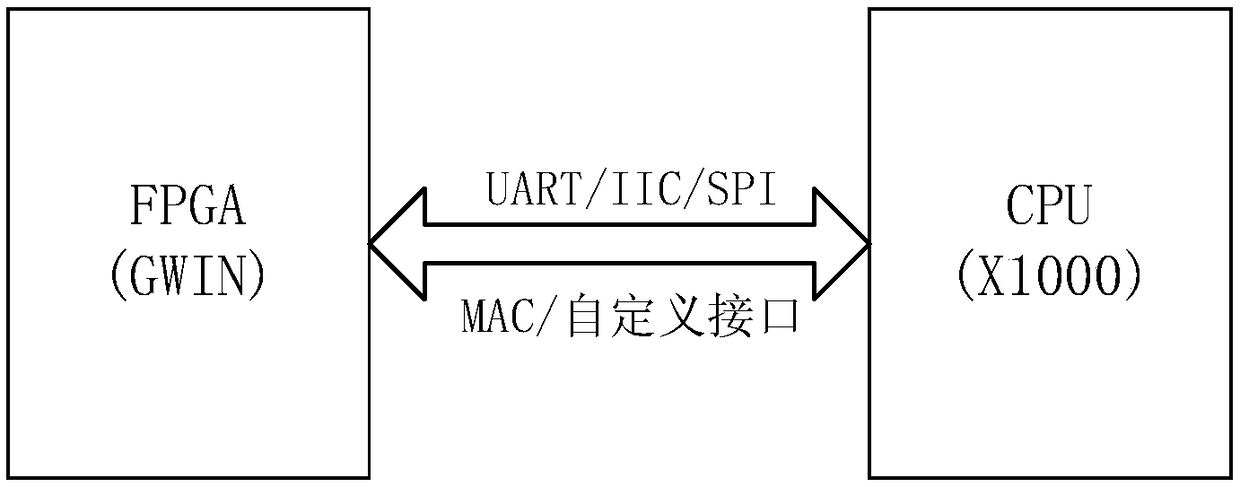
[0120] Wherein, the FPGA, as a slave device, does not have an interface protocol IP core, and the FPGA defines a SDIO communication interface and adopts the SDIO communication protocol.

[0121] Furthermore, FPGA adopts Gaoyun's GW1N-18 device.

[0122] In summary, the FPGA code...

Embodiment 2

[0124] SDIO communication interface realization device between a kind of FPGA and CPU, see Figure 5 , the device includes: FPGA as a slave device, FPGA includes:

[0125] The first verification module 1 is used to perform CRC7 verification on the received command packet;

[0126] The sending module 2 is used to send a response, and add a CRC7 check result at the end of the response data packet;

[0127] The storage module 3 is used to store an SDIO register table for initialization of SDIO communication;

[0128] The second check module 4 is used to perform CRC16 check on the received data, and transmit the check result in the form of interruption;

[0129] The data sending module 5 is used to send data to the CPU, and add the CRC16 check result at the end of the data.

[0130] To sum up, the FPGA-customized SDIO communication interface provided by the embodiment of the present invention adopts the SDIO communication protocol, and communicates with the CPU through the SDIO...

Embodiment 3

[0132] A method for realizing SDIO communication interface between FPGA and CPU, see Image 6 , CPU as master device, the method comprises the following steps:

[0133] 201: The CPU completes the loading of platform devices and drivers; completes the detection of SDIO devices, completes the SDIO initialization, and adds SDIO device nodes; the CPU obtains the bus device driver process, and completes the registration and detection of the SDIO bus;

[0134] 202: The CPU registers the SDIO device driver process, which is used to match with the SDIO device and complete the registration and loading of the driver; the CPU registers a hybrid device for access by the application program.

[0135] Further, driver registration includes:

[0136] 1) Functions for realizing platform device registration and functions for realizing platform driver registration;

[0137] 2) It is used to realize the function of detecting SDIO equipment; it is used to realize the addition of SDIO nodes;

[...


PUM


Abstract

The invention discloses an FPGA (field programmable gate array) and CPU (central processing unit) SDIO (secure digital input output) communication interface implementation method and device. An FPGA serves as a slave device without an IP (interface protocol) core, customizes an SDIO communication interface and adopts an SDIO communication protocol. A CPU serves as a master device, acquires a hybrid device drive process matched with an SDIO device and finishes drive registration and loading. The CPU can register one hybrid device in a drive, so that an application program can access the hybriddevice. The communication interface is applicable to the CPU and the FPGA in most design, and can meet the communication requirements of non-high-speed interfaces.

Description

technical field [0001] The present invention relates to the application technical field of FPGA and CPU data communication interface, relate in particular to a kind of SDIO (secure digital input and output) communication interface realization method and device between FPGA and CPU. Background technique [0002] FPGAs have been more and more widely used in various electronic products. The prices of FPGAs from different manufacturers and models vary greatly, and the interfaces supported by the IP cores of FPGAs are also different. [0003] At the same time, the support of the CPU to the communication protocol is also limited. Some communication interfaces between FPGA and CPU have a rate too low to meet application requirements, and some protocols are complex and difficult to implement on the FPGA side. [0004] Therefore, in the actual use process, how to ensure high communication rate and low bit error rate, how to improve code portability and communication reliability have...

Claims


Application Information

Patent Timeline
Patent Type & Authority Applications(China)
IPC IPC(8): G06F9/4401G06F11/10
CPCG06F9/4411G06F11/1004
Inventor 毕顺利唐占涛吴淑艳苏锦秀郭建岩张长利孟祥臣袁静
Owner JUNENG SPECIAL COMM EQUIP CO LTD TOEC GRP
Why Eureka
Try Eureka