Pixel compensating circuit, drive method thereof, and AMOLED display panel

A compensation circuit and display panel technology, applied in static indicators, instruments, etc., can solve problems such as reducing the life of pixel compensation circuits, achieve the effect of improving display effect and quality, and prolonging service life

Active Publication Date: 2018-11-30
WUHAN CHINA STAR OPTOELECTRONICS SEMICON DISPLAY TECH CO LTD
View PDF10 Cites 10 Cited by
  • Summary
  • Abstract
  • Description
  • Claims
  • Application Information

AI Technical Summary

Problems solved by technology

However, when the luminescence signal EM(n) is at a high potential, T1 still works normally in

Method used


Image

  • Pixel compensating circuit, drive method thereof, and AMOLED display panel
  • Pixel compensating circuit, drive method thereof, and AMOLED display panel
  • Pixel compensating circuit, drive method thereof, and AMOLED display panel

Examples


Embodiment Construction

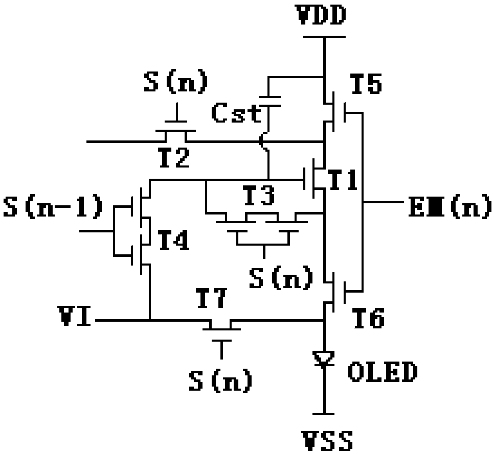
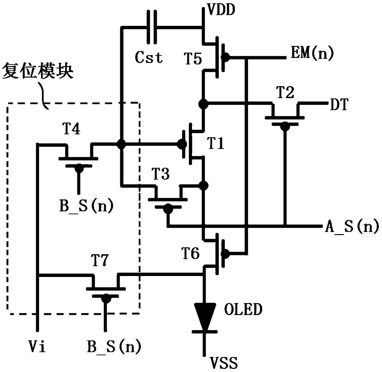
[0053] The present invention provides a pixel compensation circuit, which is applied to an AMOLED display panel, such as image 3 As shown, the pixel compensation circuit includes a light emitting device, a reset module, a storage capacitor Cst, a first thin film transistor T1, a second thin film transistor T2, a third thin film transistor T3, a fifth thin film transistor T5 and a sixth thin film transistor T6. Here, the light emitting device may be an OLED device.

[0054] Both ends of the storage capacitor Cst are connected to the drain of the fifth TFT T5 and the gate of the first TFT T1 respectively.

[0055] The drain and the gate of the fifth TFT T5 are respectively connected to the power supply voltage signal VDD and the light emitting signal EM(n), and the source of the fifth TFT T5 is connected to the drain of the first TFT T1.

[0056] The source of the first thin film transistor T1 is connected to the drain of the sixth thin film transistor T6, the source of the si...


PUM


Abstract

The invention provides a pixel compensating circuit. The pixel compensating circuit comprises a reset module, a storage capacitor, a first thin film transistor, a fifth thin film transistor and a sixth thin film transistor, wherein the reset module resets a grid electrode of the first thin film transistor and an anode of a light-emitting device according to the control of a second scanning signal;a data signal and a first scanning signal access into a drain electrode and a grid electrode of a second thin film transistor, respectively; the first scanning signal accesses into a grid electrode of a third thin film transistor; and the first scanning signal comprises one or at least two continuous pulses in one frame of time, meanwhile, when an AMOLED display panel needs black frame insertion,one black frame insertion time interval exists between the first pulse of the first scanning signal and the pulse of the second scanning signal, and when the second scanning signal contains at leasttwo continuous pulses in one frame of time, the at least two continuous pulses correspond to the pulse of a data signal. With the technical scheme provided by the invention, the service life of the pixel compensating circuit can be prolonged, and the display quality of the display panel is promoted.

Description

technical field [0001] The invention relates to the field of display technology, in particular to a pixel compensation circuit, a driving method thereof, and an AMOLED display panel. Background technique [0002] OLED (Organic Light-Emitting Diode, organic light-emitting diode) display panel has the advantages of wide color gamut, high contrast, energy saving, foldability, etc., so it has strong competitiveness in the new era of display. AMOLED (Active-matrix organic light emitting diode, active matrix organic light-emitting diode) display technology is one of the key development directions of flexible display. The basic driving circuit of an AMOLED display is 2T1C, which includes a switching thin film transistor, a driving thin film transistor and a storage capacitor Cst. Since the threshold voltage Vth of the driving thin film transistor tends to drift, the driving current of the OLED fluctuates, which causes defects in the OLED display panel and affects image quality. I...

Claims


Application Information

Patent Timeline
IPC IPC(8): G09G3/3225
CPCG09G3/3225
Inventor 曾勉
Owner WUHAN CHINA STAR OPTOELECTRONICS SEMICON DISPLAY TECH CO LTD
Why Eureka
Try Eureka