Photosensitive assembly and preparation method thereof, array substrate and display device

A technology of photosensitive components and photodiodes, which is applied in the direction of electrical components, electric solid devices, semiconductor devices, etc., can solve the problems of affecting the contrast of fingerprints, the small signal-to-noise ratio of photodiodes, and the effect of photodiodes on fingerprint recognition, etc., so as to improve the contrast , Improve the detection effect and improve the accuracy

Inactive Publication Date: 2018-11-30
BOE TECH GRP CO LTD
View PDF4 Cites 6 Cited by
  • Summary
  • Abstract
  • Description
  • Claims
  • Application Information

AI Technical Summary

Problems solved by technology

[0004] However, due to the large dark current in the PN junction in the photosensitive sensing layer, the signal-to-noise ratio of the photodiode is too small,

Method used


Image

  • Photosensitive assembly and preparation method thereof, array substrate and display device
  • Photosensitive assembly and preparation method thereof, array substrate and display device
  • Photosensitive assembly and preparation method thereof, array substrate and display device

Examples


Embodiment Construction

[0030] The following will clearly and completely describe the technical solutions in the embodiments of the present invention with reference to the accompanying drawings in the embodiments of the present invention. Obviously, the described embodiments are only some, not all, embodiments of the present invention. Based on the embodiments of the present invention, all other embodiments obtained by persons of ordinary skill in the art without making creative efforts belong to the protection scope of the present invention.

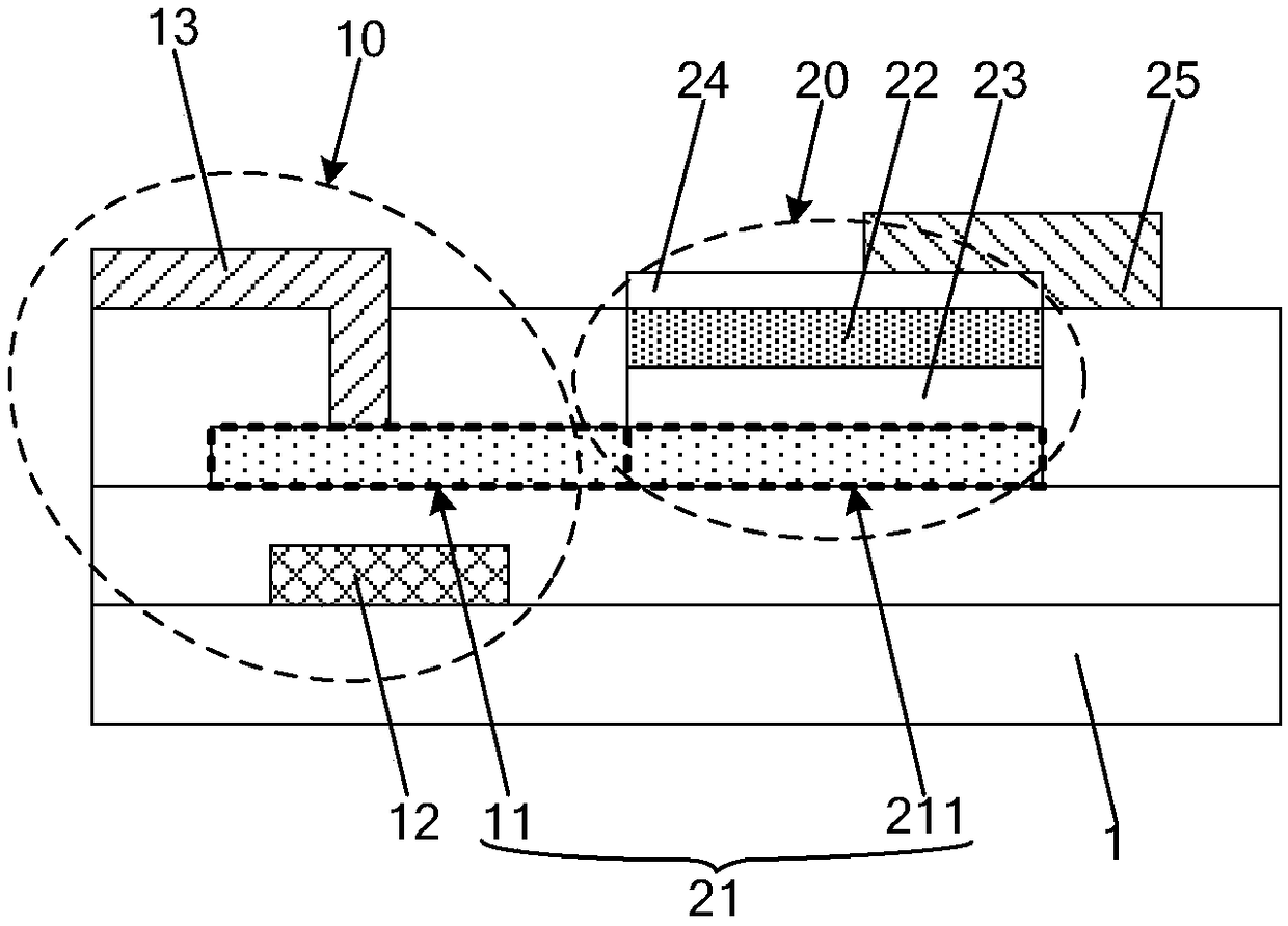
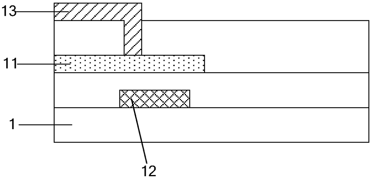
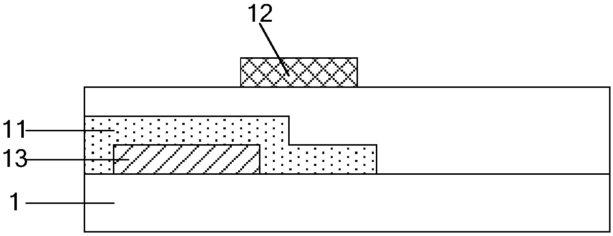
[0031] An embodiment of the present invention provides a photosensitive component, such as figure 1 As shown, it includes: a switch unit 10, the switch unit 10 includes an active layer 11; a photodiode 20, the photodiode 20 includes a P-type semiconductor layer 22 and an N-type semiconductor layer 21 that are stacked, wherein the N-type semiconductor layer 21 includes an The opposite portion facing the P-type semiconductor layer 22 and the extension portion ex...


PUM


Abstract

The embodiment of the invention provides a photosensitive assembly and a preparation method thereof, an array substrate and a display device, and relates to the technical field of displaying. A dark current of photodiode can be reduced, and the detection effect of the photodiode can be improved. The photosensitive assembly comprises a switching unit comprising an active layer, and the photodiode;the photodiode comprises a P-type semiconductor layer and an N-type semiconductor layer which are arranged in a stacked mode; the N-type semiconductor layer comprises a direct facing part directly facing the P-type semiconductor layer, and an extension part extending from the direct facing part out of the boundary of the P-type semiconductor layer; and at least part of the extension part is used as the active layer.

Description

technical field [0001] The invention relates to the field of display technology, in particular to a photosensitive component, a preparation method thereof, an array substrate, and a display device. Background technique [0002] Fingerprint recognition refers to identification by comparing the detailed feature points of different fingerprints. There are three main ways to realize fingerprint recognition: capacitive, optical and ultrasonic. [0003] Among them, the principle of optical fingerprint recognition is: after the light shines on the finger, it is reflected by the trough (hereinafter referred to as the valley) and the peak (hereinafter referred to as the ridge) of the finger, and shines on the photosensitive sensing layer. Fingerprint identification is performed according to the difference of received light energy. [0004] However, due to the large dark current in the PN junction in the photosensitive sensing layer, the signal-to-noise ratio of the photodiode is too...

Claims


Application Information

Patent Timeline
IPC IPC(8): H01L27/32G06K9/00
CPCG06V40/1318H10K59/60
Inventor 任庆荣宁策王珂胡合合
Owner BOE TECH GRP CO LTD
Why Eureka
Try Eureka