COF preparation method

A technology of temporary substrates and flexible films, which is applied in semiconductor/solid-state device manufacturing, electrical components, electric solid-state devices, etc., can solve the problems that the precision cannot meet the development needs of the display device field, and the precision is poor, so as to improve the effective utilization rate and reliability. Good bending ability and high precision effect

Inactive Publication Date: 2018-12-07
TRULY SEMICON
View PDF6 Cites 4 Cited by
  • Summary
  • Abstract
  • Description
  • Claims
  • Application Information

AI Technical Summary

Problems solved by technology

[0003] At present, COF is mainly prepared by TAPE process. However, the precision of this material process is poor. Generally, the minimum pitch of single-sided COF Film is 25um, and the minimum pitch of double-sided COF Film is 35um. Such precision is increasingly unable to meet the needs of display devices. development needs of the field

Method used


Image

  • COF preparation method
  • COF preparation method

Examples


Embodiment 1

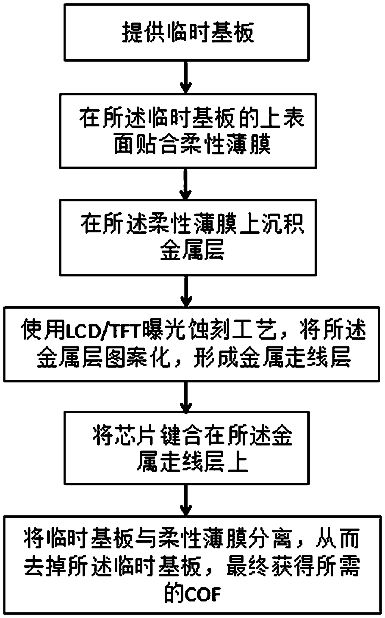
[0028] figure 1 A flow chart of a COF preparation method provided by the present invention is shown. This embodiment is a COF preparation method for single-layer wiring. Specifically, the COF preparation method includes the following steps:

[0029] (a) provision of temporary substrates;

[0030] (b) pasting a flexible film on the upper surface of the temporary substrate;

[0031] (c) depositing a metal layer on said flexible film;

[0032] (d) using an LCD / TFT exposure etching process to pattern the metal layer to form a metal wiring layer;

[0033] (e) Bonding the chip on the metal wiring layer;

[0034] (f) Separating the temporary substrate from the flexible film, thereby removing the temporary substrate and finally obtaining the desired COF.

[0035] It is worth noting that the present invention uses the LCD / TFT exposure etching process to replace the traditional TAPE process, so that the final circuit has higher precision and better flexibility, and improves the ef...

Embodiment 2

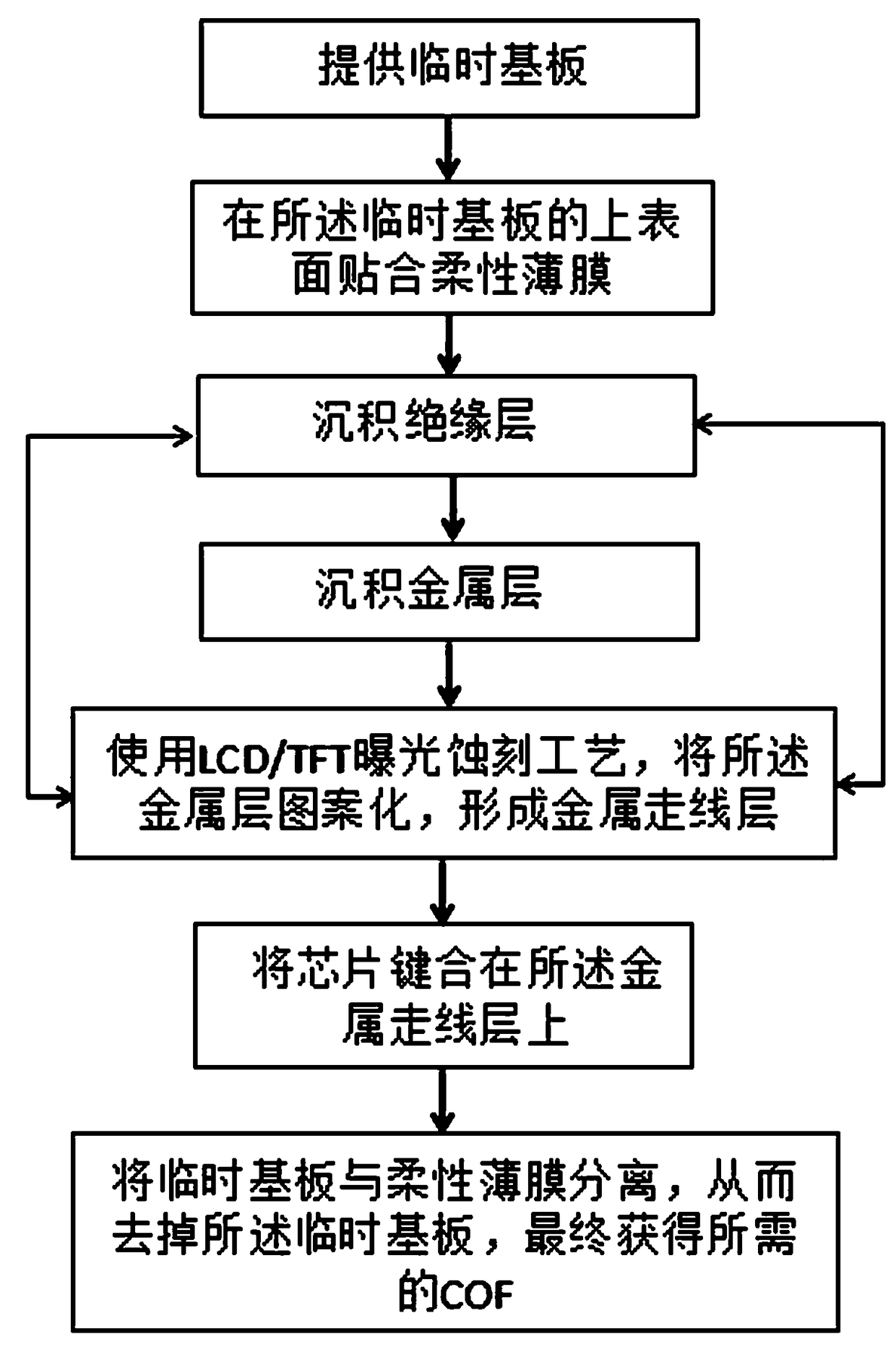
[0041] figure 2 A flow chart of a COF preparation method provided by another embodiment of the present invention is shown. This embodiment is a COF preparation method for multi-layer routing. Specifically, the COF preparation method includes the following steps:

[0042] (a) provision of temporary substrates;

[0043] (b) pasting a flexible film on the upper surface of the temporary substrate;

[0044] (c1) Deposit the insulating layer first;

[0045] (c2) depositing a metal layer on the insulating layer;

[0046] (d) using an LCD / TFT exposure etching process to pattern the metal layer to form a metal wiring layer;

[0047] Repeat the above steps (c1), (c2) and (d) according to the predetermined number of times;

[0048] (e) Bond the chip on the metal wiring layer;

[0049] (f) Separating the temporary substrate from the flexible film, thereby removing the temporary substrate and finally obtaining the desired COF.

[0050] It should be noted that the LCD / TFT exposure ...


PUM


Abstract

The invention discloses a COF preparation method. The method comprises: step a, providing a temporary substrate; step b, pasting a flexible film on the upper surface of the temporary substrate; step c, depositing a metal layer on the flexible film; step d, carrying out patterning on the metal layer by using an LCD/TFT exposure etching process to form a metal wiring layer; step e, bonding a chip tothe metal wiring layer; and step f, separating the temporary substrate from the flexible film to remote the temporary substrate, thereby obtaining a needed COF. Therefore, the process precision is improved; the flexibility and bending ability are enhanced; the application range is large; and the cost is low.

Description

technical field [0001] The invention relates to the field of chip packaging, in particular to a COF preparation method. Background technique [0002] COF (Chip On Film) refers to chip-on-film bonding packaging, which is widely used in the field of display devices. With the rapid development of the electronics and communication industries, the demand for displays is increasing day by day, and related products are all light, thin, short, and small. This requires high density, small volume, and free installation. A new generation of packaging technology to meet the above requirements. It is against this background that COF technology develops rapidly and becomes a main packaging form of driver ICs for flat panel displays such as LCD and PDP, and then becomes an important part of these display modules. COF technology has become one of the mainstream trends in driver IC packaging for future flat panel displays. [0003] At present, COF is mainly prepared by TAPE process. Howev...

Claims


Application Information

Patent Timeline
Patent Type & Authority Applications(China)
IPC IPC(8): H01L21/48H01L23/492H01L21/56
CPCH01L21/4846H01L21/561H01L23/492
Inventor 廖亿彬吴振忠刘秀霞何基强
Owner TRULY SEMICON
Why Eureka
Try Eureka