A semiconductor chip packaging array

A chip packaging and semiconductor technology, applied in semiconductor devices, semiconductor/solid-state device manufacturing, semiconductor/solid-state device components, etc., can solve problems such as poor soldering performance, increase yield, increase area, and improve soldering performance Effect

Active Publication Date: 2020-12-25
NANTONG TONGFU MICROELECTRONICS CO LTD
View PDF10 Cites 0 Cited by
  • Summary
  • Abstract
  • Description
  • Claims
  • Application Information

AI Technical Summary

Problems solved by technology

[0003] The inventors of the present application have found in the long-term research process that in the process of soldering existing semiconductor chip packaging devices (for example, quad flat no-lead package devices, square flat no-lead package devices, etc.), soldering often occurs. A case of poor performance because the leads of existing semiconductor packages have only a small area on the bottom for solder to climb

Method used


Image

  • A semiconductor chip packaging array
  • A semiconductor chip packaging array
  • A semiconductor chip packaging array

Examples


Embodiment Construction

[0036] The following will clearly and completely describe the technical solutions in the embodiments of the present application with reference to the drawings in the embodiments of the present application. Obviously, the described embodiments are only some of the embodiments of the present application, not all of them. Based on the embodiments in this application, all other embodiments obtained by persons of ordinary skill in the art without making creative efforts belong to the scope of protection of this application.

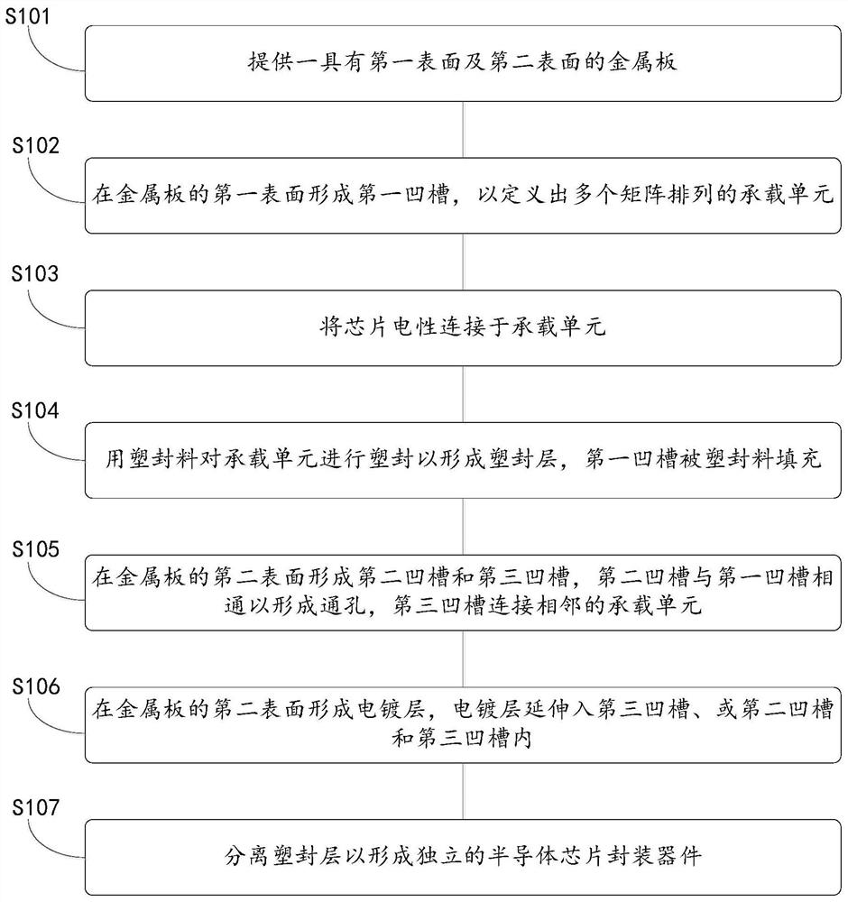
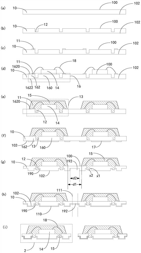
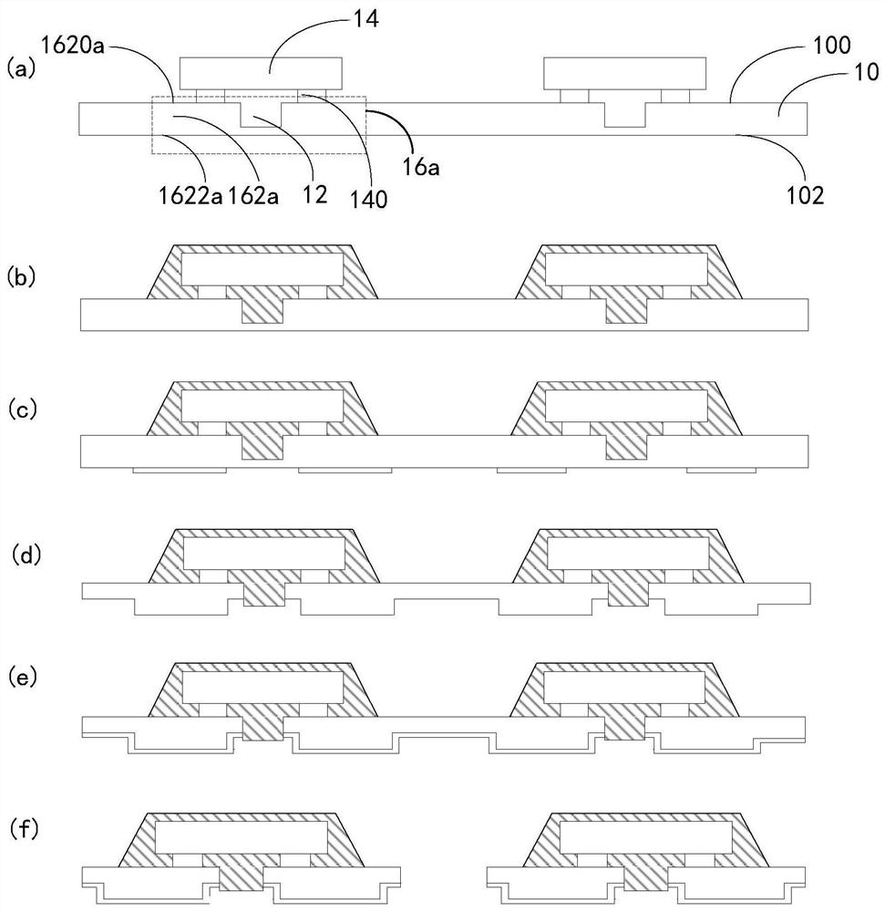
[0037] see Figure 1-Figure 2 , figure 1 It is a schematic flow diagram of an embodiment of the semiconductor chip packaging method of the present application, figure 2 for figure 1 A schematic structural diagram of an embodiment corresponding to steps S101-S107, image 3 for figure 1 A schematic structural diagram of another embodiment corresponding to steps S103-S107, Figure 4 for figure 1 A schematic structural diagram of another embodiment correspo...


PUM


Abstract

The present application discloses a semiconductor chip package array, which includes: a lead frame, the lead frame includes: a plurality of matrix-arranged carrying units, a first groove extending from the first surface of the lead frame to the second surface, a first groove extending from the second surface A second groove extending to the first surface, a third groove extending from the second surface to the first surface, wherein the first groove communicates with the second groove to form a through hole, and the third groove connects adjacent The carrying unit; the chip, the chip is arranged on the carrying unit, and is electrically connected with the carrying unit; the plastic sealing layer, the plastic sealing compound wraps the chip and at least part of the carrying unit, and the first groove is filled with the plastic sealing compound to form the plastic sealing layer; electroplating layer, and the electroplating layer is disposed on the second surface of the lead frame and extends into the third groove, or the third groove and the second groove. Through the above method, the present application can increase the area of ​​the pins of the semiconductor package array for soldering to climb.

Description

technical field [0001] The present application relates to the technical field of semiconductor chips, in particular to a packaging array of semiconductor chips. Background technique [0002] With the rapid development of science and technology, the research and development and production of semiconductor chip packaging devices are constantly developing towards the direction of high density, high performance, high reliability and low cost. As a result, the volume of the semiconductor chip packaging device is continuously reduced, the number of pins arranged on the semiconductor chip packaging device is greatly increased, the distance between the pins is getting smaller and smaller, and the density of the pins is getting higher and higher. [0003] The inventors of the present application have found in the long-term research process that in the process of soldering existing semiconductor chip packaging devices (for example, quad flat no-lead package devices, square flat no-lea...

Claims


Application Information

Patent Timeline
Patent Type & Authority Patents(China)
IPC IPC(8): H01L23/495
CPCH01L23/49548H01L23/49582H01L21/4832H01L21/561H01L23/3107H01L24/16H01L24/45H01L24/48H01L24/85H01L24/97H01L2224/13099H01L2224/16245H01L2224/32245H01L2224/45111H01L2224/45124H01L2224/45138H01L2224/45144H01L2224/45147H01L2224/45155H01L2224/4516H01L2224/45171H01L2224/45565H01L2224/48091H01L2224/48247H01L2224/73265H01L2224/81447H01L2224/81455H01L2224/8146H01L2224/85401H01L2224/85418H01L2224/85447H01L2224/85455H01L2224/85471H01L2224/97H01L2924/181H01L2924/00014H01L2924/00012H01L2224/85H01L2224/81H01L2924/013H01L2924/01024H01L2924/01026H01L2924/01014H01L2924/01028H01L2924/01029H01L2924/0105H01L2924/01048H01L21/4825H01L21/4828H01L21/565H01L21/78H01L23/49503H01L23/49513H01L23/4952H01L23/49575H01L23/562H01L24/32H01L2224/48175
Inventor 石磊
Owner NANTONG TONGFU MICROELECTRONICS CO LTD
Why Eureka
Try Eureka