Pulse shift circuit and frequency synthesizer

A pulse shifting and circuit technology, applied in phase shifter, pulse processing, pulse shaping, etc., can solve the problem of pulse signal output time shift

Active Publication Date: 2018-12-21
MITSUBISHI ELECTRIC CORP
View PDF8 Cites 0 Cited by
  • Summary
  • Abstract
  • Description
  • Claims
  • Application Information

AI Technical Summary

Problems solved by technology

That is, the conventional pulse shift circuit shifts the reset timing of the pulse shift circuit by the number of clocks corresponding to the shift amount from the reset timing of the reference pulse circuit, thereby shifting the output timing of the pulse signal.

Method used


Image

  • Pulse shift circuit and frequency synthesizer
  • Pulse shift circuit and frequency synthesizer
  • Pulse shift circuit and frequency synthesizer

Examples


Embodiment approach 1

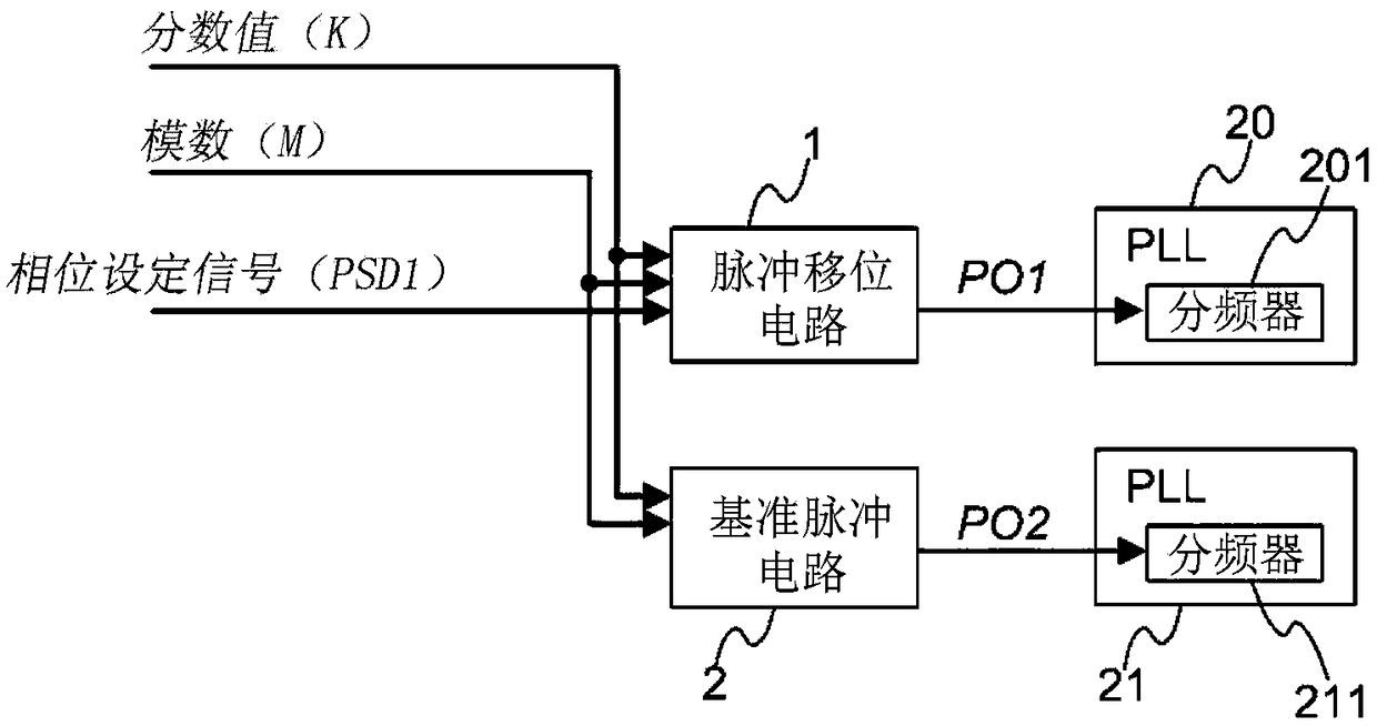
[0031] figure 1 It is a diagram showing an example of use of the pulse shift circuit according to Embodiment 1 of the present invention.

[0032] exist figure 1 Among them, pulse shift circuit 1, PLL 20, reference pulse circuit 2 and PLL 21 constitute a frequency synthesizer capable of controlling the phase difference of two PLL output signals. The pulse shift circuit 1 is connected to a frequency divider 201 built in the PLL 20 . The reference pulse circuit 2 is connected to a frequency divider 211 built in the PLL 21 . K (an example of the first signal) is frequency setting data and is generally called a fractional value. M (an example of the second signal) is frequency setting data and is generally called a modulus. PO1 and PO2 are the frequency division number control signals of the frequency divider 201 and the frequency divider 211 respectively, and are pulse signals output according to the cycle of M / K. The values ​​below the decimal point of the frequency division...

Embodiment approach 2

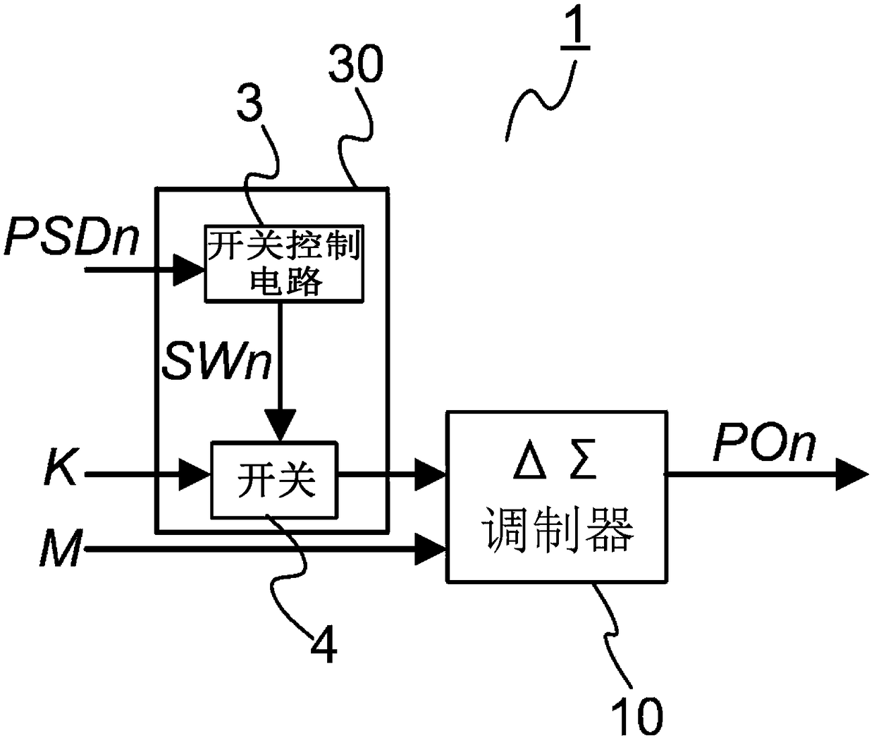
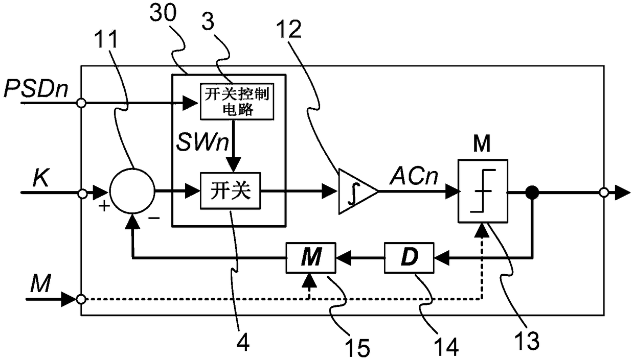
[0066] Embodiment 1 shows a circuit configuration in which, in the pulse shift circuit, the signal input to the integrator 12 of the ΔΣ modulator 10 is held constant for several clocks according to the phase setting signal, thereby realizing frequency division. The shift of the digital control signal (PO1). Here, a circuit configuration is shown in which the frequency division number control signal is shifted with one clock in the pulse shift circuit. Accordingly, the operating time of the circuit can be reduced, and an effect of reducing power consumption of the circuit can be obtained.

[0067] Figure 6 It is a configuration diagram showing a configuration example of a pulse shift circuit according to Embodiment 2 of the present invention. The input signal control circuit 31 is different from the pulse shift circuit 1 of the first embodiment in that it is composed of an addition bit generation circuit 5 and an adder 6 .

[0068] The addition bit generation circuit 5 is a...

Embodiment approach 3

[0081] In Embodiment 1, the case where K of the pulse shift circuit is fixed is shown. Here, the case where K of the pulse shift circuit changes with time is shown. Thus, in an F-PLL that generates an FM (Frequency Modulation: Frequency Modulation) signal such as a chirp signal, pulse shifting for phase difference control can be realized.

[0082] Figure 9 It is a configuration diagram showing a configuration example of a pulse shift circuit according to Embodiment 3 of the present invention. The pulse shift circuit of Embodiment 3 is the same as that of Embodiment 1 figure 2 The input side of the shown pulse shift circuit 1 has an FM control circuit 41 , an integrator 42 and an addition circuit 43 .

[0083] The FM control circuit 41 is an FM control circuit that outputs a derivative amount of K corresponding to a frequency change amount in FM. For example, the FM control circuit 41 uses a logic circuit of FPGA.

[0084] The integrator 42 is an integrator that integrat...


PUM


Abstract

A problem with conventional distortion pulse shift circuits is that the output timing of a pulse signal cannot be controlled unless a reset signal is used. A pulse shift circuit is provided with: an integrator which integrates an input first signal at each clock; a quantizer into which a second signal is input, and which outputs a pulse signal when the integrated value from the integrator is equalto the signal value of the second signal or exceeds the signal value of the second signal; a delay circuit which delays the pulse signal; a converter which is provided at a stage preceding or following the delay circuit and which converts the signal value of the pulse signal into the signal value of the second signal; a subtractor which subtracts the signal value of the pulse signal, converted bythe converter, from the signal value of the first signal to be input into the integrator; and an input signal control circuit into which a third signal is input, which is disposed at a stage preceding the integrator, and which either adds a signal value corresponding to the third signal to the first signal to be input into the integrator, or blocks input of the first signal into the integrator for a number of clocks corresponding to the third signal.

Description

technical field [0001] The present invention relates to pulse shifting circuits. Background technique [0002] Fractional N PLL (Phase Locked Loop: Phase Locked Loop) can control the frequency division number of the frequency divider by using the frequency division number control signal generated by the ΔΣ modulator, and lock the PLL with the frequency division number below the decimal point. [0003] In addition, when two fractional N PLLs with the same configuration are connected in parallel and the same reference signal is input to the parallel PLLs, the frequency division control signal generated by the ΔΣ modulator is adjusted by clock units. With respect to one shift, a phase difference can be given between the output signals of the two PLLs according to the amount of shift. [0004] A pulse shift circuit described in Non-Patent Document 1 is known as a circuit that shifts a frequency division control signal generated by a ΔΣ modulator in units of clocks. [0005] A ...

Claims


Application Information

Patent Timeline
Patent Type & Authority Applications(China)
IPC IPC(8): H03L7/197H03L7/23H03M3/02
CPCH03K5/01H03K2005/00013H03K2005/00286H03L7/1976H03L7/23H03M7/3028
Inventor 中沟英之桧枝护重水谷浩之田岛贤一
Owner MITSUBISHI ELECTRIC CORP
Why Eureka
Try Eureka