A packaging method and packaging structure for an image sensor chip

A technology for image sensor chips and packaging methods, which is applied in radiation control devices, semiconductor devices, electrical components, etc., and can solve the problem of high difficulty in image sensor chip packaging, complicated procedures, and bonding of image sensor chips and light-transmitting cover plates High precision requirements and other issues, to achieve the effect of simplifying the forming process, reducing the difficulty of packaging, and reducing the bonding accuracy

Active Publication Date: 2021-07-09
CHINA WAFER LEVEL CSP
View PDF3 Cites 0 Cited by
  • Summary
  • Abstract
  • Description
  • Claims
  • Application Information

AI Technical Summary

Problems solved by technology

However, limited by the packaging structure and its forming process, the plastic sealing layer in the prior art needs multiple injection molding processes, which not only complicates the process, but also requires relatively high bonding accuracy between the image sensor chip and the light-transmitting cover plate. High, making the packaging of image sensor chips more difficult

Method used


Image

  • A packaging method and packaging structure for an image sensor chip
  • A packaging method and packaging structure for an image sensor chip
  • A packaging method and packaging structure for an image sensor chip

Examples


Embodiment Construction

[0079] The following will clearly and completely describe the technical solutions in the embodiments of the application with reference to the drawings in the embodiments of the application. Apparently, the described embodiments are only some of the embodiments of the application, not all of them. Based on the embodiments in this application, all other embodiments obtained by persons of ordinary skill in the art without making creative efforts belong to the scope of protection of this application.

[0080] In order to make the above objects, features and advantages of the present application more obvious and comprehensible, the present application will be further described in detail below in conjunction with the accompanying drawings and specific implementation methods.

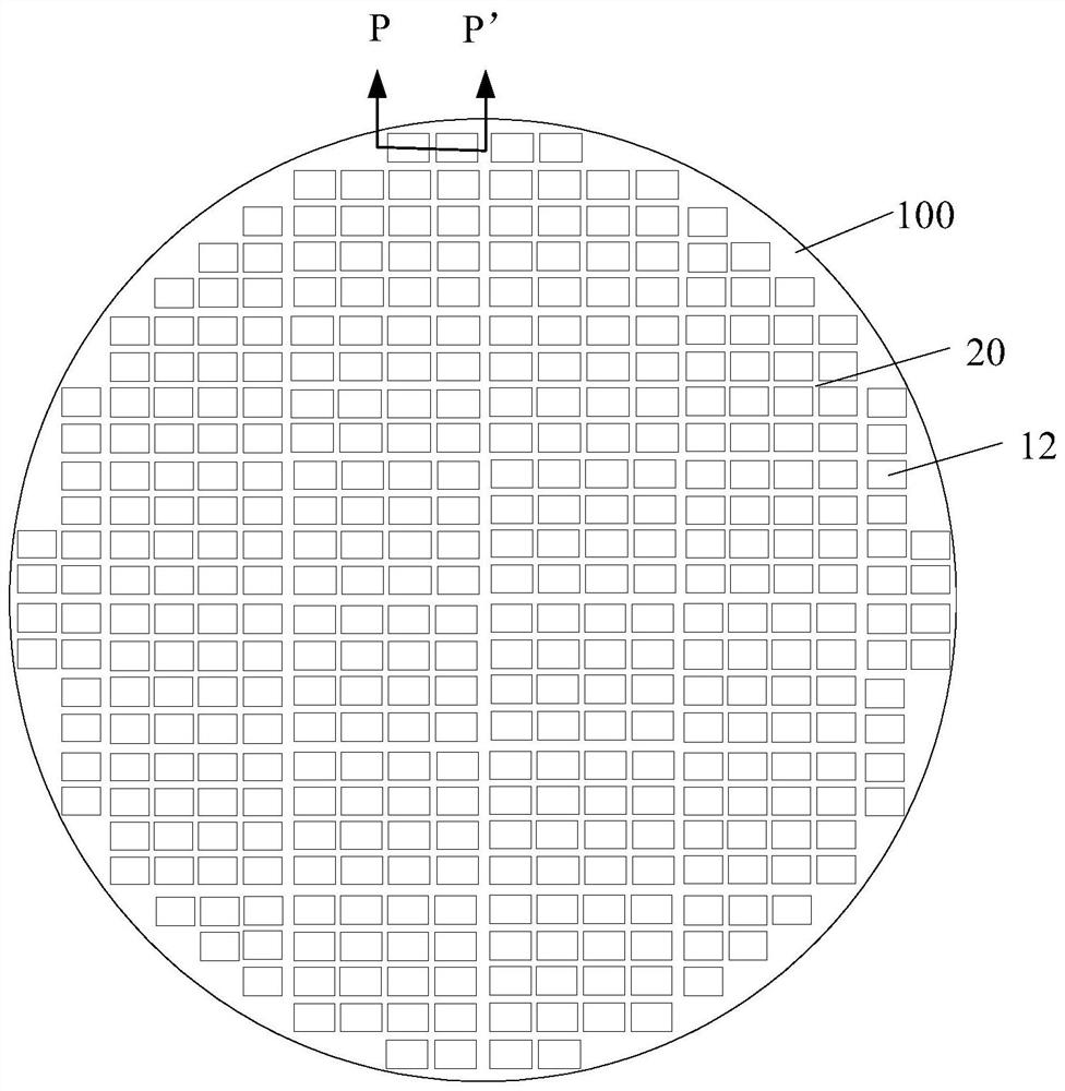
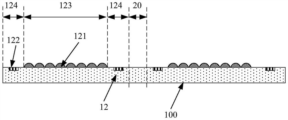
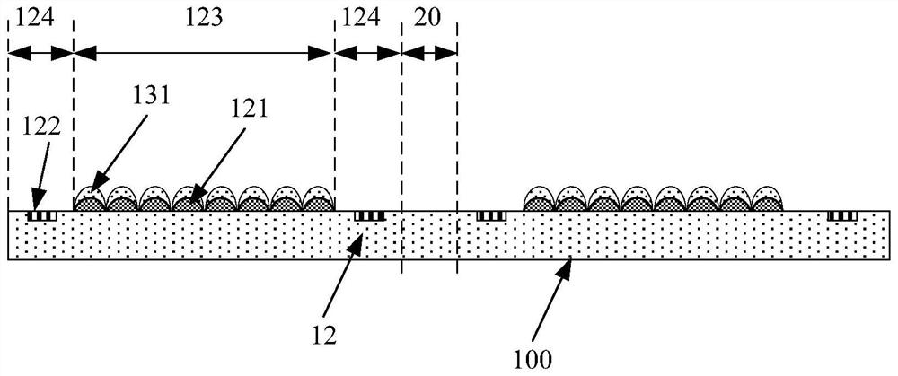
[0081] refer to Figure 1-Figure 17 , Figure 1-Figure 17 It is a schematic diagram of the preparation process of the packaging method of the image sensor chip provided in the embodiment of the present applic...


PUM

PropertyMeasurementUnit
thicknessaaaaaaaaaa
thicknessaaaaaaaaaa
thicknessaaaaaaaaaa

Abstract

The present application discloses a packaging method and packaging structure of an image sensor chip, wherein, in the packaging method of the image sensor chip, during the bonding process of the transparent cover plate and the substrate, the first part of the transparent cover plate is An adhesive film layer completes the photosensitive area and the non-photosensitive area, so that a cavity-free structure is formed between the light-transmitting cover plate and the image sensor chip, ensuring sufficient adhesion between the light-transmitting cover plate and the image sensor chip Therefore, during the subsequent injection molding process of a single image sensor chip and substrate to form a plastic seal layer, due to the strong bonding strength between the light-transmitting cover plate and the image sensor chip, multiple injection moldings are not required The plastic sealing layer can be directly formed at one time, which not only simplifies the forming process of the plastic sealing layer, but also does not need to control the first adhesive film layer only on the periphery of the photosensitive area, which reduces the bonding accuracy of the image sensor chip and the light-transmitting cover plate , thereby reducing the packaging difficulty of the image sensor chip.

Description

technical field [0001] The present application relates to the technical field of optical detection devices, and more specifically, to a packaging method and packaging structure for an image sensor chip. Background technique [0002] An image sensor chip is an electronic device that senses external light and converts it into an electrical signal. Image sensor chips are usually fabricated using semiconductor manufacturing processes. After the image sensor chip is manufactured, a packaged package structure is formed by performing a series of packaging processes on the image sensor chip to be used in electronic devices such as digital cameras and digital video cameras. [0003] When packaging the image sensor chip, it is necessary to first bond the image sensor chip to the light-transmitting cover plate, and then carry out processes such as wire bonding and plastic sealing to realize the packaging of the image sensor chip and improve the quality of the image sensor chip. Excel...

Claims


Application Information

Patent Timeline
Patent Type & Authority Patents(China)
IPC IPC(8): H01L27/146
CPCH01L27/14601H01L27/14632H01L27/14683
Inventor 王之奇
Owner CHINA WAFER LEVEL CSP
Why Eureka
Try Eureka