PCB (printed circuit board) cleaning tooling

A PCB board and tooling technology, which is applied in the field of PCB board cleaning tooling, can solve the problems of increased production costs, high labor intensity, and low production efficiency of printed circuit boards.

Active Publication Date: 2019-01-04
ANHUI SHENZE ELECTRONICS TECH
View PDF7 Cites 8 Cited by
  • Summary
  • Abstract
  • Description
  • Claims
  • Application Information

AI Technical Summary

Problems solved by technology

[0003] In the process of producing printed circuit boards, oxides or pollutants that reduce the service life of printed circuit boards will remain on the printed circuit boards, so it is necessary to clean the printed circuit boards to enhance the service life of printed circuit boards Or reduce the probability of damage and corrosion of printed circuit boards. At present, some printed circuit boards need to be cleaned manually, which is too labor-intensive and the cleaning efficiency is too low. The printed circuit board is damaged, which reduces the utilization rate of the printed circuit board, which makes the production efficiency of the printed circuit board too low in the production process and increases the production cost.

Method used


Image

  • PCB (printed circuit board) cleaning tooling
  • PCB (printed circuit board) cleaning tooling
  • PCB (printed circuit board) cleaning tooling

Examples


Embodiment 1

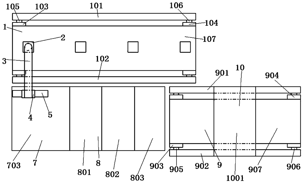
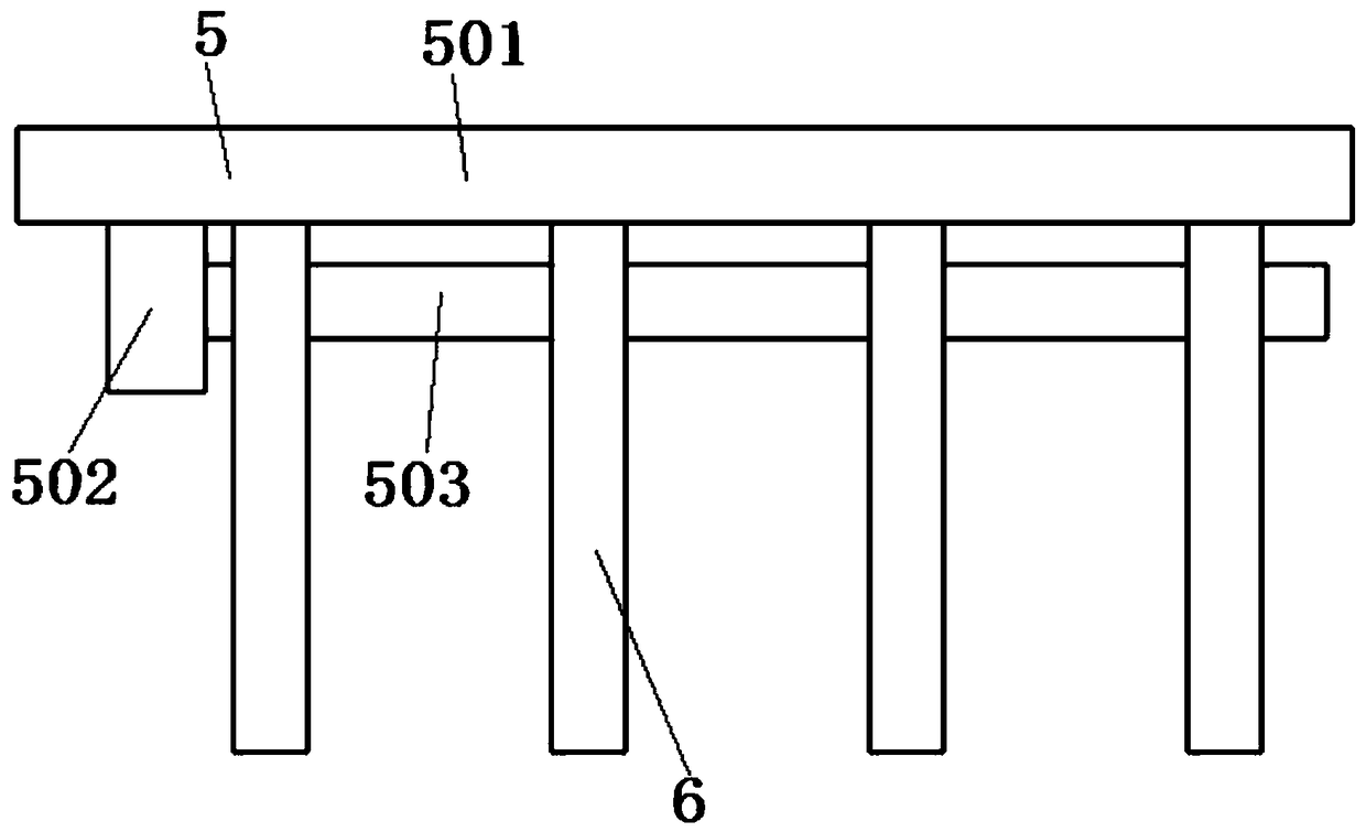
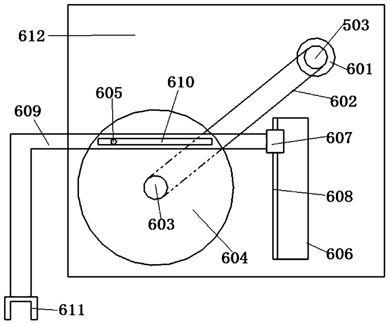
[0027] A PCB board cleaning tool, including a first conveyor belt component 1, a connecting block 2, an L-shaped connecting rod 3, an electric telescopic push rod 4, a clamping component 5, a lifting and clamping component 6, a water cleaning component 7, and a rinsing component 8 , the second transmission belt assembly 9 and the warm air drying assembly 10, the first conveyor belt assembly 1 is evenly provided with a plurality of connecting blocks 2, the connecting block 2 is connected with an L-shaped connecting rod 3, and the other end of the L-shaped connecting rod 3 is on the lower side An electric telescopic push rod 4 is connected, the telescopic end of the electric telescopic push rod 4 is connected with a clamping part 5, a plurality of lifting clamping assemblies 6 are arranged under the clamping part 5, and a water cleaning assembly 7 is arranged under the clamping part 5, The front side of the water cleaning assembly 7 is provided with a first conveyor belt assembly...


PUM


Abstract

The invention discloses a PCB (printed circuit board) cleaning tooling which comprises a first conveyor belt assembly, wherein a plurality of connecting blocks are uniformly arranged on the first conveyor belt assembly; an L-shaped connecting rod is connected onto one connecting block; an electric telescopic push rod is connected with the lower side of the other end of the L-shaped connecting rod;a clamping part is connected with the telescopic end of the electric telescopic push rod; a plurality of lifting clamping assemblies are arranged under the clamping part; a water cleaning assembly isarranged below the clamping part; the first conveyor belt assembly is arranged on the front side of the water cleaning assembly; a rinsing assembly and a second transmission belt assembly are sequentially arranged on the right side of the water cleaning assembly; and a warm air drying assembly is arranged on the second transmission belt assembly. The PCB cleaning tooling disclosed by the invention has the beneficial effects that through the lifting clamping assemblies, the water cleaning assembly, the rinsing assembly and the warm air drying assembly, pollutants on both sides of a PCB can bemore quickly cleaned up; the quicker and cleaner rinsing operation can be facilitated; and by the utilization of vertical-downward airflow generated by a warm air blower and rotating fan blades, the deep cleaning and drying treatment of the PCB can be facilitated.

Description

technical field [0001] The invention belongs to the technical field of printed circuit boards, and in particular relates to a cleaning tool for PCB boards. Background technique [0002] Printed circuit board (PCB circuit board), also known as printed circuit board, is called "printed" circuit board because it is made by electronic printing. A printed circuit board is a substrate for assembling electronic components, and is a printed board that forms point-to-point connections and printed components on a general-purpose substrate according to a predetermined design. The main function of this product is to make various electronic components form a predetermined circuit connection and play the role of relay transmission. It is a key electronic interconnection of electronic products. [0003] In the process of producing printed circuit boards, oxides or pollutants that reduce the service life of printed circuit boards will remain on the printed circuit boards, so it is necessar...

Claims


Application Information

Patent Timeline
Patent Type & Authority Applications(China)
IPC IPC(8): B08B5/02B08B3/04B08B1/02F26B21/00
CPCB08B1/02B08B3/041B08B5/023F26B21/00
Inventor 张雷赵守江姜广彪张琳胡洪波
Owner ANHUI SHENZE ELECTRONICS TECH
Why Eureka
Try Eureka