A method and apparatus for evaluating semiconductor reliability

A reliability and semiconductor technology, applied in special data processing applications, instruments, electrical digital data processing, etc., can solve the problems of shortened update cycle and unacceptable reliability test.

Pending Publication Date: 2019-01-04
洪启集成电路(珠海) 有限公司
View PDF1 Cites 6 Cited by
  • Summary
  • Abstract
  • Description
  • Claims
  • Application Information

AI Technical Summary

Problems solved by technology

To make matters worse, traditional time-consuming reliability testing is increasi...

Method used


Image

  • A method and apparatus for evaluating semiconductor reliability
  • A method and apparatus for evaluating semiconductor reliability
  • A method and apparatus for evaluating semiconductor reliability

Examples


Embodiment Construction

[0199] The technical solutions of the present invention will be described in further detail below in conjunction with the accompanying drawings and specific embodiments.

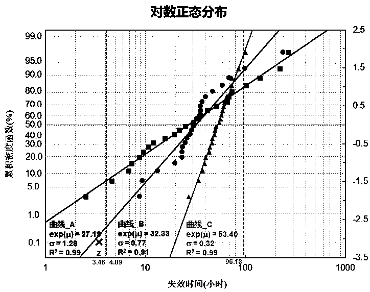
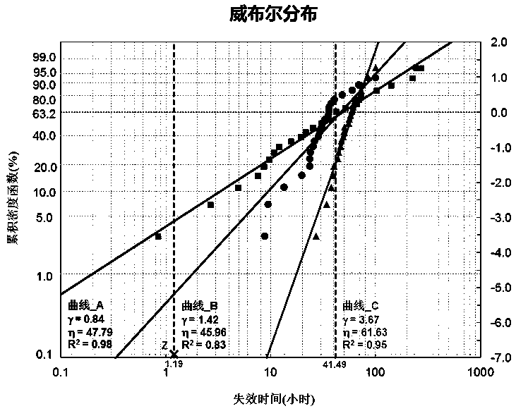
[0200] In practice, when almost identical devices are subjected to the same stress conditions, most of the time they do not fail at the same time due to differences in material microstructure and manufacturing process. Therefore, in the semiconductor reliability evaluation of the present invention, not only Time To Failure (TTF) is of interest, but more precisely, the distribution of Time To Failure is of interest. This reflects the main difference between the present invention and the methods proposed in previous reliability demonstration experiments. Traditionally, two probability density functions have been widely applied to failures in the semiconductor industry: the lognormal and the Weibull distribution. The Weibull distribution is often used to model phenomena that exhibit extreme behavior that encom...


PUM


Abstract

The invention provides a method and apparatus for rapid reliability evaluation of semiconductor, including an efficient and reliable reliability reference (BL) management system and a test scheme baseon sequential probability ratio test (SPRT). In order to ensure the credibility of the SPRT test scheme, the Bayesian approach is used to update the BL database continuously. This is the first time that the SPRT has been applied to reliability risk assessment with two unknown parameters. By using the method and the device provided by the invention, the reliability of the semiconductor can be quickly measured, and the sample size and the test time can be reduced.

Description

technical field [0001] The invention relates to the technical field of semiconductors, in particular to a semiconductor reliability evaluation method and device. Background technique [0002] Semiconductor manufacturing, as one of the most complex processes in modern industry, contains hundreds of complex process steps, including photolithography, etching, thin film, diffusion and cleaning. These processes can usually be divided into two parts: Front-End of Line (FEOL) and Back-End of Line (BEOL). The FEOL process is usually defined as starting from the wafer and ending when the metal wire connection begins . Transistors are made in FEOL, which has quite a lot of diffusion process to form eg well junction, field isolation and determine the source / drain (S / D) field of the transistor. Gate oxide, as one of the most critical features, is grown after S / D formation, followed by the formation of polysilicon and inter-level dielectrics (Inter-Level Dielectrics, ILD). At BEOL, si...

Claims


Application Information

Patent Timeline
IPC IPC(8): G06F17/50
CPCG06F30/367
Inventor 不公告发明人
Owner 洪启集成电路(珠海) 有限公司
Why Eureka
Try Eureka