
Pixel circuit and driving method thereof and display panel

A driving method and technology of pixel circuits, applied in static indicators, instruments, etc., can solve problems such as leaving horizontal stripes

Active Publication Date: 2019-01-04
BOE TECH GRP CO LTD +1
View PDF10 Cites 2 Cited by
  • Summary
  • Abstract
  • Description
  • Claims
  • Application Information

AI Technical Summary

Problems solved by technology

[0007] In view of this, an embodiment of the present invention provides a pixel circuit, its driving method and a display panel to solve the problem that the existing driving method leaves horizontal stripes

Method used


Image

  • Pixel circuit and driving method thereof and display panel
  • Pixel circuit and driving method thereof and display panel
  • Pixel circuit and driving method thereof and display panel

Examples


Embodiment Construction

[0049] The specific implementations of the pixel circuit provided by the embodiments of the present invention, its driving method and the display panel will be described in detail below with reference to the accompanying drawings.

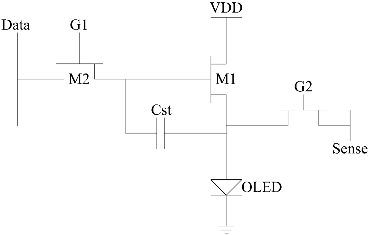
[0050] A driving method for a pixel circuit provided in an embodiment of the present invention is based on Figure 6a and Figure 6b For the illustrated pixel circuit with external compensation, for the convenience of description, the display time of each frame is now divided into a light-emitting time period and a blank time period, and the blank time period is divided into: the first time period, the second time period, The third time period, the fourth time period and the fifth time period; the specific driving method is as follows Figure 4 As shown, the following steps may be included:

[0051] S401. In the first time period, apply a first turn-on signal to the first scan signal terminal, apply a second turn-on signal to the second scan sign...


PUM


Abstract

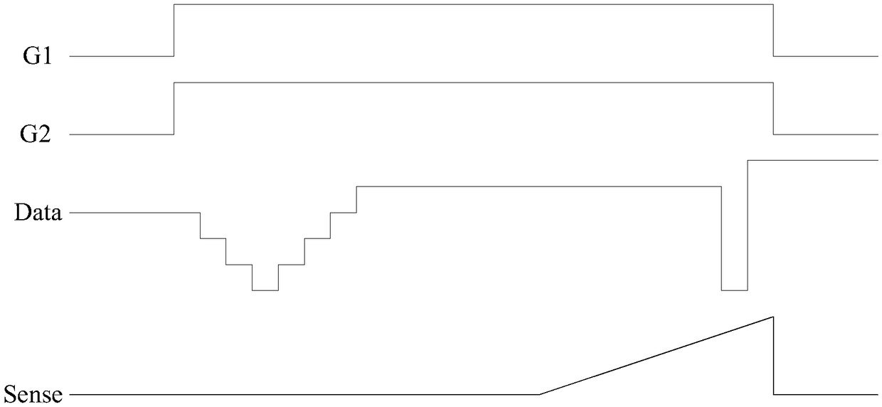
The invention discloses a pixel circuit and a driving method thereof and a display panel. Firstly a zero voltage signal is loaded to the data signal end for eliminating the influence of conduction ofthe first switching transistor and the second switching transistor on the gate voltage of the driving transistor under the effect of the parasitic capacitance in the blank period of time; then a firstlevel data signal of a certain duration is loaded to the data signal end so as to eliminate the hysteresis effect of the driving transistor from the turn-off to conduction process by using the bias algorithm; then a falling data signal is loaded to the data signal end to eliminate the influence of factors such as data coupling; then a second level data signal is maintained on the data signal endduring acquisition of the compensation data, and the induction signal end is charged after the first switching transistor is turned off for acquisition of compensation data of the induction signal end; and finally a gain data signal is load to the data signal end to eliminate scanning dark lines so as to eliminate the problem of horizontal stripes left in switching of frames.

Description

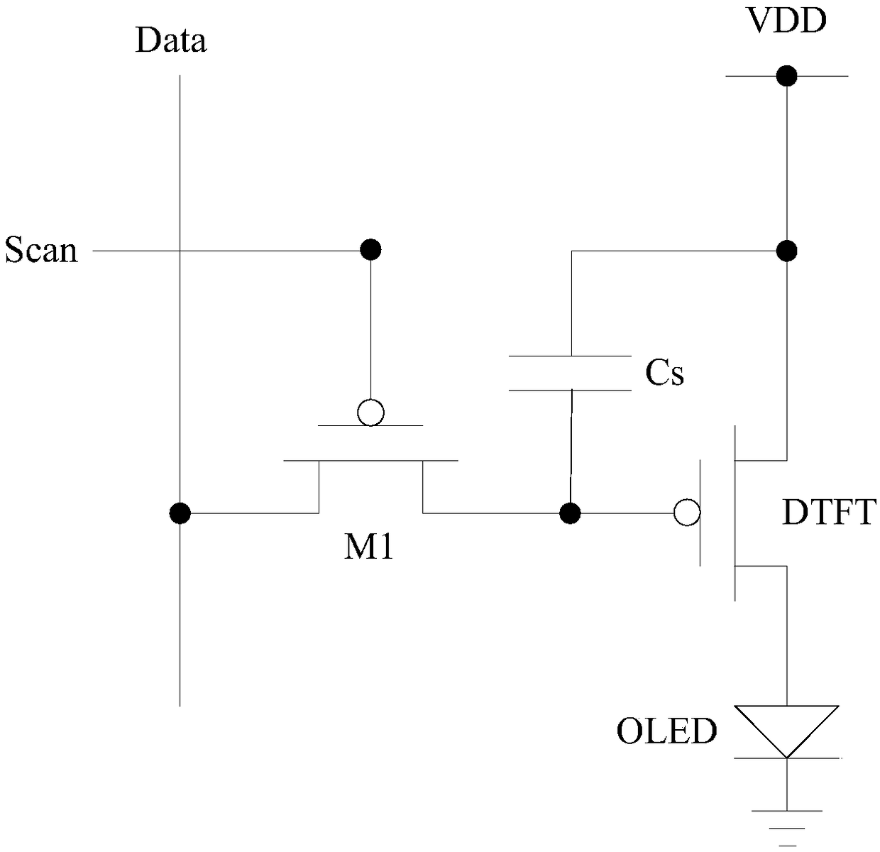
technical field [0001] The invention relates to the field of display technology, in particular to a pixel circuit, a driving method thereof and a display panel. Background technique [0002] Organic Light Emitting Diode (OLED) display is one of the hot spots in the field of flat panel display research today. Compared with liquid crystal display, OLED display has low energy consumption, low production cost, self-illumination, wide viewing angle and fast response speed. At present, OLED displays have begun to replace traditional Liquid Crystal Displays (LCDs) in flat panel display fields such as mobile phones, PDAs, and digital cameras. Among them, pixel circuit design is the core technical content of OLED display, which has important research significance. [0003] Unlike LCDs that use voltage to control brightness, OLEDs are driven by current and need to use current to control light emission. For example, in the existing 2T1C pixel circuit, such as figure 1 As shown, the ...

Claims


Application Information

Patent Timeline
IPC IPC(8): G09G3/3233
CPCG09G3/3233G09G3/20G09G2320/029G09G2310/08G09G2320/0295G09G2300/0819G09G2300/0842G09G2320/043G09G2320/045G09G2320/0233G09G3/3275G09G3/3258G09G3/3266G09G2310/061
Inventor 徐海侠吴月袁粲鲍文超
Owner BOE TECH GRP CO LTD
Learn More