
Method for preparing a carrier for a photoconductor for the formation of an electrophotographic recording element and a recording element formed accordingly

Inactive Publication Date: 2005-01-06
EASTMAN KODAK CO
View PDF13 Cites 1 Cited by
  • Summary
  • Abstract
  • Description
  • Claims
  • Application Information

AI Technical Summary

Benefits of technology

[0011] The underlying objective of the invention is to avoid the aforementioned problems, and particularly to reduce, point injections, hysteresis effects, dependence upon environmental conditions, especially moisture, and / or interference patterns.

Problems solved by technology

In comparison to OPC layers, coatings made of a-Si have a higher wear resistance, but are burdened with higher production costs.
Toner particles consequently, tend to adhere to non-imaged areas that have no electrostatic latent image, so that defective images are created, namely, “fuzzy” images.
This surface structure in turn leads to charge injection and charge collapse, which cause image defects, particularly, if the thickness of the blocking layer (or “barrier layer”) is significantly less than 1 μm.
As a result, these light portions interfere with each other, which can lead to interference rings, depending upon variations in layer thickness.
These types of interference rings lead to an irregular print density.

Method used


Image

  • Method for preparing a carrier for a photoconductor for the formation of an electrophotographic recording element and a recording element formed accordingly
  • Method for preparing a carrier for a photoconductor for the formation of an electrophotographic recording element and a recording element formed accordingly

Examples


Embodiment Construction

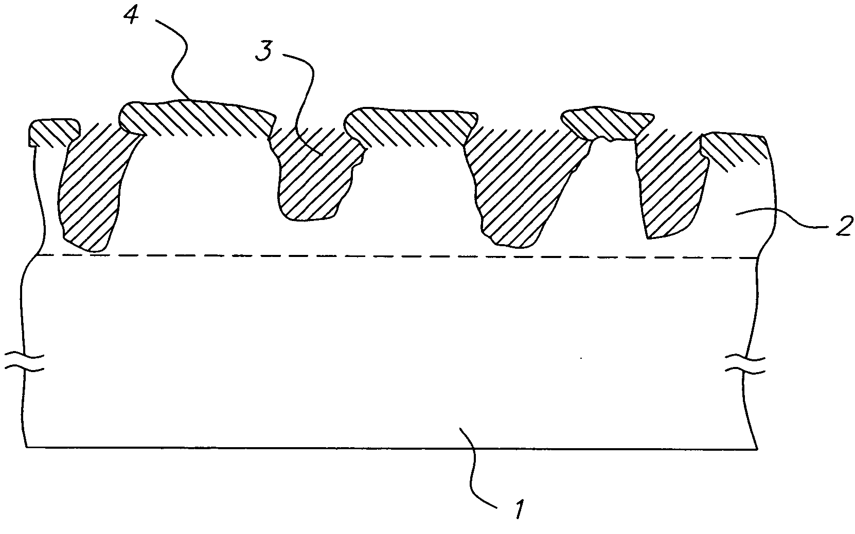
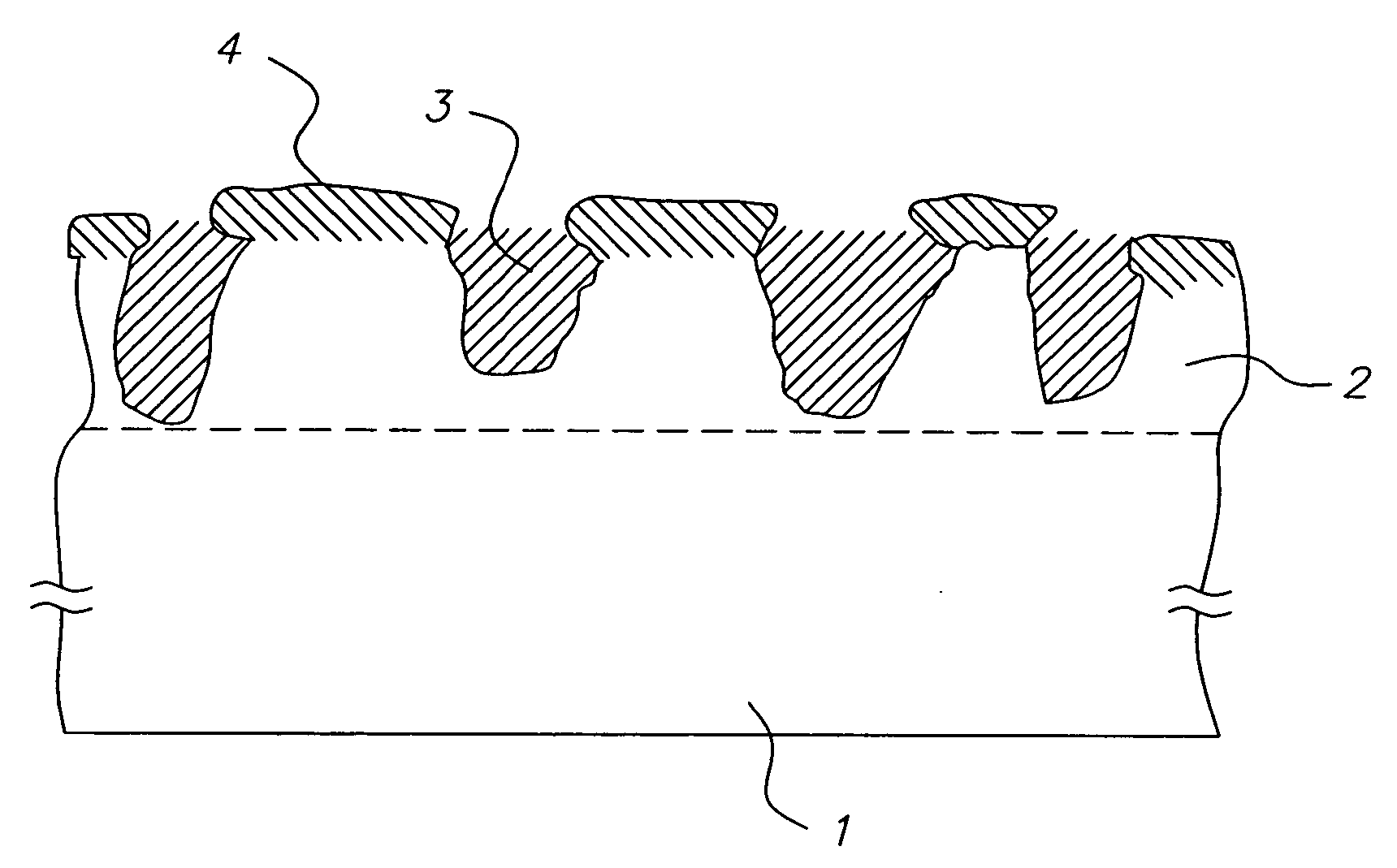
[0014] In the figure, a substrate 1, or a substrate layer made of aluminum, for example, of a photoconductor of a strip, of a cylinder, or of a collar, for instance, is depicted. This substrate 1 is initially oxidized, for example, by etching or anodizing, and is thus provided with an oxide layer 2 made of Al2O3, for example. As shown and described above, this inorganic blocking or barrier oxide layer 2, is non-homogenous and craterlike or cavernous. In order to level the craters in the oxide layer 2, the craters are preferably filled with a cold water-based impregnating agent 3 that is used, for example, for the conservation of archeological findings, particularly those findings made of wood, as disclosed in U.S. Pat. No. 6,022,589, issued on Feb. 8, 2000, in the name of Jerome M. Klosowski et al.

[0015] Subsequently, for additional oxidation, the surface that is filled with the impregnating agent 3 is rinsed with preferably, warm water that is enriched with ozone (O2 and / or O3), s...


PUM

PropertyMeasurementUnit
Lengthaaaaaaaaaa
Lengthaaaaaaaaaa

Abstract

A carrier or substrate for a photoconductor to be used for the formation of an electrophotographic recording element, particularly an imaging drum for an electrophotographic printing press, wherein the carrier is made of a metal or a metal alloy, preferably of aluminum, is prepared wherein the surface of the carrier supporting the photoconductor, used to form a barrier layer, is oxidized, preferably by etching and / or anodizing. The oxidized surface of the barrier layer is sealed with a sealing material following oxidation, and a preservative or impregnating agent is used as the sealing material.

Description

FIELD OF THE INVENTION [0001] The invention relates to an electrophotographic recording element, and a method for preparing a carrier or substrate for a photoconductor for the formation of an electrophotographic recording element, particularly, an imaging drum for an electrophotographic printing press, wherein the carrier is made of a metal or a metal alloy, preferably of aluminum, and the surface of the carrier supporting the photoconductor, which is used to form a barrier layer, is oxidized, preferably by etching and / or anodizing, preferably to a barrier layer thickness of approximately 0.05 μm to approximately 1.5 μm and wherein the oxidized surface of the barrier layer is sealed with a sealing material following oxidation. BACKGROUND OF THE INVENTION [0002] For the electrophotographic process, the formation of the photoconducting recording element, which can also be called photo carrier or imaging unit, is particularly important. The basic principle of electrophotography can her...

Claims


Application Information

Patent Timeline
IPC IPC(8): C25D11/24G03G5/10G03G5/14
CPCC25D11/246G03G5/102G03G2215/00957G03G5/144G03G5/104
Inventor DRAGER, UDOSCHULZE-HAGENEST, DETLEF
Owner EASTMAN KODAK CO
Learn More