Multi-wafer stack structure and forming method thereof

一种堆叠结构、晶圆的技术,应用在电气元件、电固体器件、电路等方向,能够解决硅基板不能适应共用焊盘的需求、厚度限制要求、整体厚度厚等问题,达到减少堆叠厚度、厚度减小、增加封装密度的效果

Active Publication Date: 2019-01-08
WUHAN XINXIN SEMICON MFG CO LTD
View PDF11 Cites 8 Cited by
  • Summary
  • Abstract
  • Description
  • Claims
  • Application Information

AI Technical Summary

Problems solved by technology

[0003] However, the inventors found that there are some problems in the traditional multi-wafer wire interconnection method: first, there are restrictions on the thickness of multi-wafer stacking towards high-density development, and space for bonding wires needs to be reserved between multi-wafers that use wire bonding , the silicon substrate itself also has a certain thickness, and to a certain extent, the overall thickness is thicker after multi-wafer stacking; in addition, the lead wire is usually made of gold wire, which has a high cost; in addition, the silicon substrate cannot adapt to the high-density development of multi-wafer stacking. The need for more and more shared pads

Method used


Image

  • Multi-wafer stack structure and forming method thereof
  • Multi-wafer stack structure and forming method thereof
  • Multi-wafer stack structure and forming method thereof

Examples


Embodiment Construction

[0049] The manufacturing method of the semiconductor device and the semiconductor device proposed by the present invention will be further described in detail below in conjunction with the accompanying drawings and specific embodiments. The advantages and features of the present invention will become clearer from the following description. It should be noted that all the drawings are in a very simplified form and use imprecise scales, and are only used to facilitate and clearly assist the purpose of illustrating the embodiments of the present invention.

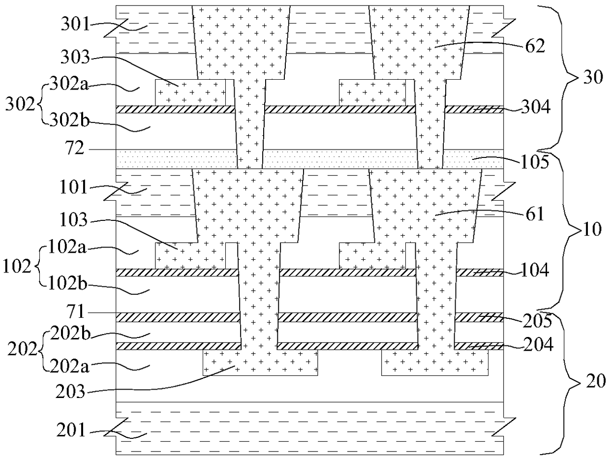
[0050] An embodiment of the present invention provides a multi-wafer stacking structure, such as figure 1 , Figure 10 and Figure 14 shown, including:

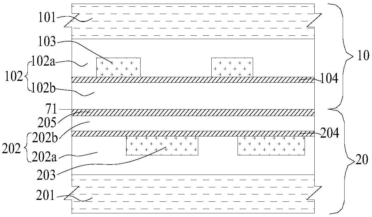
[0051] A first wafer 10, the first wafer 10 comprising a first substrate 101, a first dielectric layer 102 and a first metal layer 103;

[0052] The second wafer 20, the second wafer 20 includes a second substrate 201, a second dielectric layer 202 and a second metal lay...


PUM


Abstract

The invention provides a multi-wafer stack structure and a forming method thereof. The first dielectric layer and the second dielectric layer are bonded with each other, and the first interconnectionlayer is electrically connected with the second metal layer and the first metal layer through the first opening. The third dielectric layer and the insulating layer are bonded to each other, and the second interconnect layer is electrically connected to the third metal layer and the first interconnect layer through the second opening. The invention eliminates the need for reserving bonding lead space between wafers, eliminates silicon substrate, realizes multi-wafer interconnection and reduces the thickness of multi-wafer stack, thereby reducing the thickness of the whole device after multi-wafer stack packaging, increasing the packaging density and meeting the requirement of increasingly lightweight semiconductor products. Moreover, the semiconductor device no longer needs leads, and thedesign and processing of the silicon substrate and several common pads on the silicon substrate are omitted, which is favorable for reducing the cost and simplifying the process.

Description

technical field [0001] The invention belongs to the technical field of integrated circuit manufacturing, and in particular relates to a multi-wafer stacking structure and a forming method thereof. Background technique [0002] Under the trend of highly integrated semiconductor development, wire bonding is often used to realize the interconnection between multiple wafers after stacking multiple wafers. Specifically, multiple wafers are stacked vertically on a dedicated silicon substrate. Each wafer has multiple pads for interconnection, and there are multiple common pads on the silicon substrate. One end of the lead is bonded to the pad of the wafer, and the other end of the lead is bonded together. On the common pad of the silicon substrate, the interconnection between multiple wafers is realized. [0003] However, the inventors found that there are some problems in the traditional multi-wafer wire interconnection method: first, there are restrictions on the thickness of mu...

Claims


Application Information

Patent Timeline
Patent Type & Authority Applications(China)
IPC IPC(8): H01L23/522H01L23/528H01L21/768
CPCH01L21/76802H01L21/76877H01L23/5226H01L23/5283H01L21/76898H01L23/481H01L25/0657H01L25/50H01L2225/06544H01L21/2885H01L21/76804H01L21/7684H01L27/0688
Inventor 曾甜赵长林
Owner WUHAN XINXIN SEMICON MFG CO LTD
Why Eureka
Try Eureka