Secure testability design structure of encryption chip

A technology for encrypting chips and designing structures, which is applied in the field of testable design structures, can solve problems such as large attacks, and achieve the effect of low area overhead

Active Publication Date: 2019-01-11
CHANGSHA UNIVERSITY OF SCIENCE AND TECHNOLOGY
View PDF11 Cites 5 Cited by
  • Summary
  • Abstract
  • Description
  • Claims
  • Application Information

AI Technical Summary

Problems solved by technology

A scan-based attack is easier to execute, so it has a greater potential threat than an attack b

Method used


Image

  • Secure testability design structure of encryption chip
  • Secure testability design structure of encryption chip
  • Secure testability design structure of encryption chip

Examples


Embodiment Construction

[0016] In order to make the object, technical solution and advantages of the present invention clearer, the present invention will be further described in detail below in conjunction with the accompanying drawings and embodiments. It should be understood that the specific embodiments described here are only used to explain the present invention, not to limit the present invention.

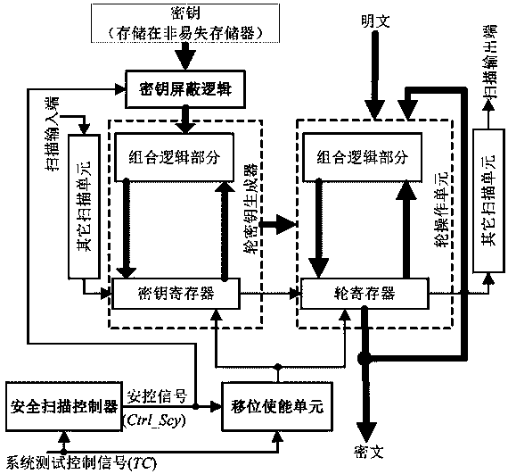
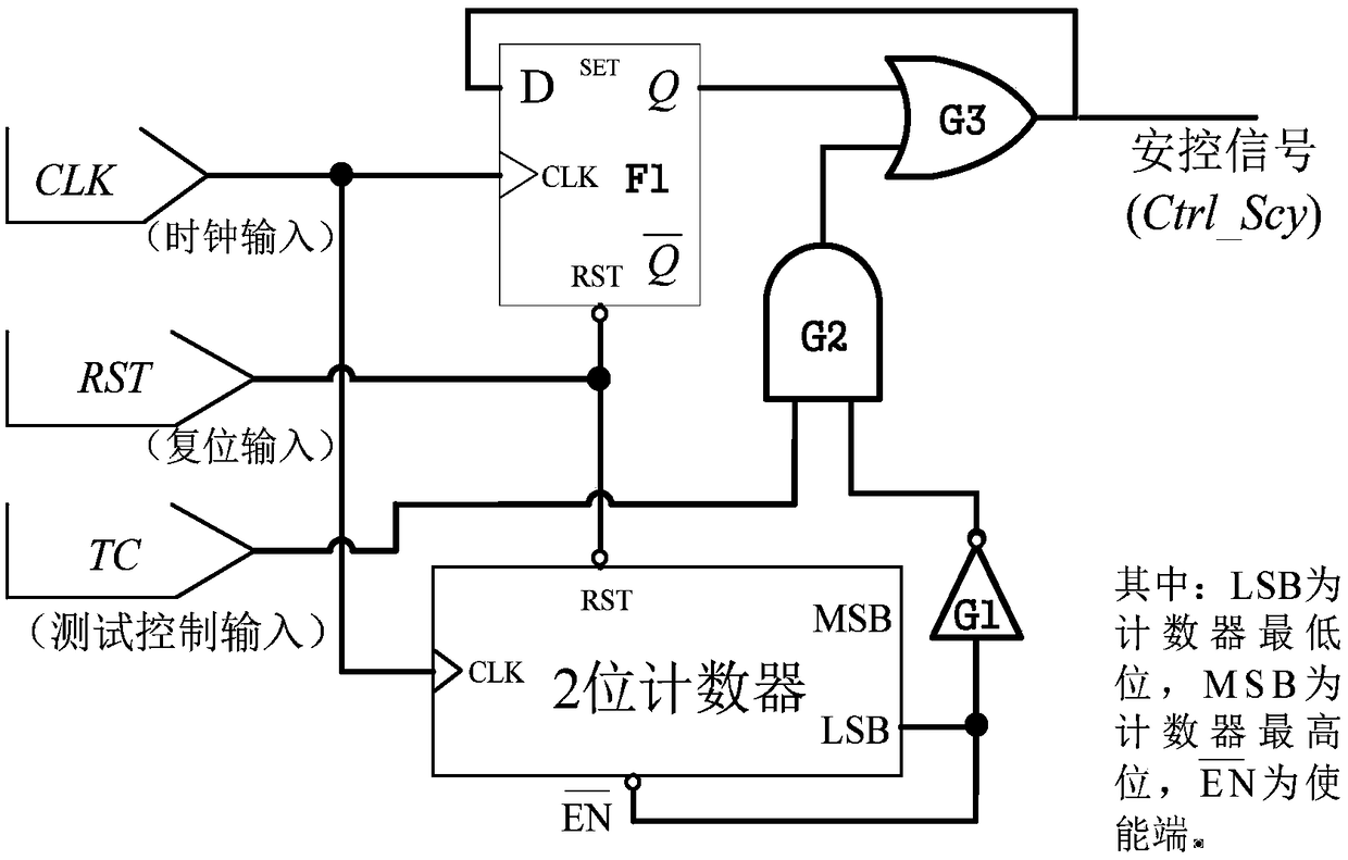
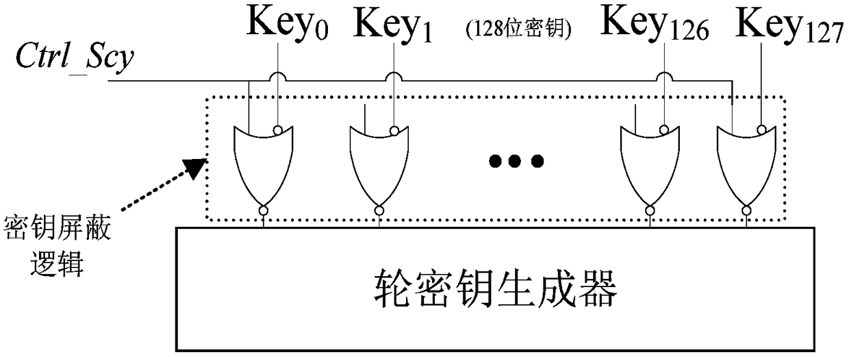
[0017] The core components of the AES encryption chip include a round operation unit and a round key generator. In the conventional scanning design, the chip key register, the wheel register in the wheel operation unit and other flip-flops are first transformed into scanning units, and then these scanning units are sequentially connected into a scanning chain. The scan chain can be used to shift in test stimuli, capture test responses, and shift out test responses under the action of test control signals. Such as figure 1 As shown, the security scanning structure of the present invention adds key...


PUM


Abstract

The invention discloses a testability design structure for protecting an encryption chip from scanning attacks. The secure testability design structure of the encryption chip is introduced with key shielding logic, shift enabling logic and a secure scan controller based on the conventional scan design structure. If the encryption chip first enters the functional mode after power-on or reset, the key shielding logic allows the key to be loaded under the control of the security scan controller, while the shift enabling logic prevents the circuit from switching to the test mode, thereby avoidingthe leakage of the encrypted information. Conversely, if the encryption chip first enters the test mode after power-on or reset, the scan shift and the response capture can be performed normally underthe control of the security scan controller, while the key is isolated, thereby ensuring that the data removed from the scan chain is independent of the key. According to the secure testability design structure of encryption chip, by adding less hardware logic, all potential scan-based side channel attacks can be resisted while ensuring the circuit testability.

Description

technical field [0001] The invention belongs to the field of hardware security, and more specifically relates to a testability design structure for protecting an encryption chip from scanning attacks. Background technique [0002] In order to protect the integrity and confidentiality of data, encryption algorithms are widely used in the field of information security, among which the Advanced Encryption Standard AES encryption algorithm is one of the most popular algorithms in symmetric key encryption. In many cases, encryption algorithms are implemented in hardware because hardware implementation has many advantages over software implementation, for example, it can provide a high data throughput rate. In hardware implementations of cryptographic algorithms, the keys are usually stored within the module and cannot be easily accessed. Since the encryption chip has zero tolerance for failure, it should be rigorously tested to ensure that it will function properly. Scanning de...

Claims


Application Information

Patent Timeline
IPC IPC(8): G01R31/28
CPCG01R31/2803
Inventor 王伟征蔡烁
Owner CHANGSHA UNIVERSITY OF SCIENCE AND TECHNOLOGY
Why Eureka
Try Eureka