An optical module

An optical module and gold finger technology, applied in the field of optical modules, can solve problems such as poor impedance matching effect of high-speed signals

Inactive Publication Date: 2019-01-15
HISENSE BROADBAND MULTIMEDIA TECH
View PDF3 Cites 10 Cited by
  • Summary
  • Abstract
  • Description
  • Claims
  • Application Information

AI Technical Summary

Problems solved by technology

[0005] The invention provides an optical module to solve the problem that the impedance matching effect of the high

Method used


Image

  • An optical module
  • An optical module
  • An optical module

Examples


Embodiment Construction

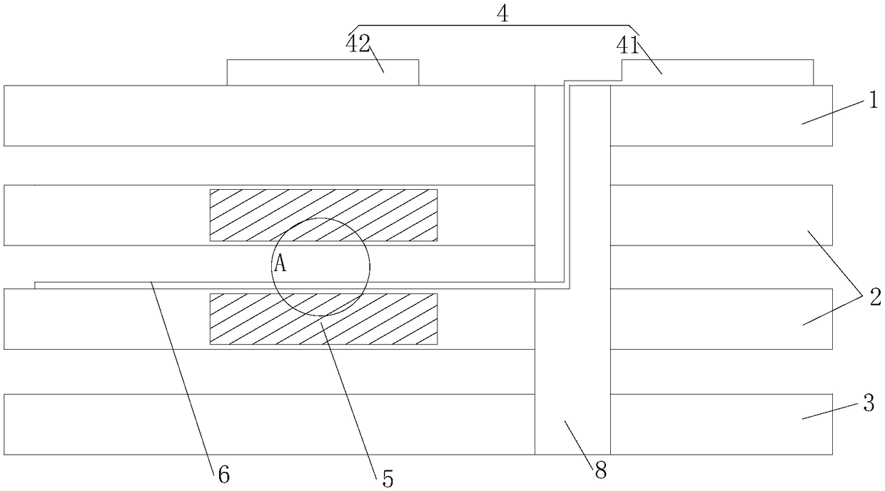
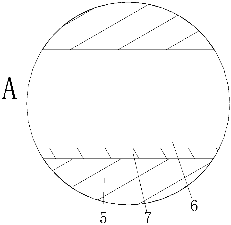
[0014] In the related art, the circuit board in the optical module generally includes a metal layer and a dielectric layer arranged between two adjacent metal layers. A first row of gold fingers and a second row of gold fingers are arranged in parallel on the surface of the top metal layer, and a high-speed signal line is arranged on the middle layer between the top layer and the last layer. The existence of high-speed signal lines makes the circuit of the circuit board a high-speed circuit. Therefore, a reference reflow layer, that is, a reference layer, is usually set under the golden finger to facilitate the transmission of high-speed signals. Usually, the metal layer closest to the golden finger is used as the reference layer of the golden finger. However, since the circuit board is thin and multi-layered, the distance between the golden finger and the reference layer is relatively short, resulting in a poor impedance matching effect for the high-speed signal transmitted i...


PUM


Abstract

An optical module is provided. The optical module includes a circuit board, wherein the circuit board includes a surface layer, a reference layer, and an intermediate layer positioned between the surface layer and the reference layer. The surface of the surface layer is provided with a first row of golden fingers and a second row of golden fingers, and the first row of golden fingers is closer tothe edge of the circuit board than the second row of golden fingers. At a projection area for by projecting that second row of goldfinger onto the intermediate layer, the intermediate layer is hollowed out to form a hollowed-out area. The hollowed-out area can be formed so that the second row of goldfingers does not flow back through the intermediate layer, but through a reference layer formed therewith, which is conducive to improving the impedance matching effect of the high-speed signal. The hollowed-out area can be formed so that the second row of goldfingers does not flow back through theintermediate layer but through a reference layer formed therewith.

Description

technical field [0001] The invention relates to the technical field of communications, in particular to an optical module. Background technique [0002] In the field of high-speed data communication, with the continuous acceleration of the communication rate, the number of communication channels for signal transmission is continuously increasing. Usually, the communication channel for high-speed signal transmission is realized through golden fingers and high-speed signal lines. In order to realize the signal transmission among the increasing high-speed signal lines, the circuit board in the optical module mostly adopts a multi-layer PCB (Printed Circuit Board, printed circuit board), and the golden fingers on the optical module mostly adopt double-row golden fingers. [0003] In the related art, the circuit board in the optical module generally includes a metal layer and a dielectric layer arranged between two adjacent metal layers. A first row of gold fingers and a second...

Claims


Application Information

Patent Timeline
IPC IPC(8): H05K1/11H05K1/02H05K1/18G02B6/42
CPCG02B6/4245G02B6/428H05K1/0298H05K1/117H05K1/18
Inventor 王欣南慕建伟王世明高庭
Owner HISENSE BROADBAND MULTIMEDIA TECH
Why Eureka
Try Eureka