
panel structure

A panel and substrate technology, applied in semiconductor/solid-state device components, semiconductor devices, electrical components, etc., can solve problems affecting the reliability of display panels, non-rectangular panel cutting cracks, performance degradation, etc., to improve resistance to external moisture Ability to invade, reduce cracking and/or flaking spots, increase the effect of moisture resistance

Active Publication Date: 2021-01-15
AU OPTRONICS CORP
View PDF3 Cites 0 Cited by
  • Summary
  • Abstract
  • Description
  • Claims
  • Application Information

AI Technical Summary

Problems solved by technology

[0003] In the current manufacturing method of display panels, the display panel is easily affected by external water vapor in the process of electronic components, such as metal oxide thin film transistors, resulting in electrical abnormalities of electronic components, thereby reducing performance
In addition, during the cutting and separation process, non-rectangular panels tend to generate stress at the edge of the display panel and cause chipping, which affects the reliability of the display panel and reduces the production yield of the display panel, increasing production costs

Method used


Image

  • panel structure
  • panel structure
  • panel structure

Examples


Embodiment Construction

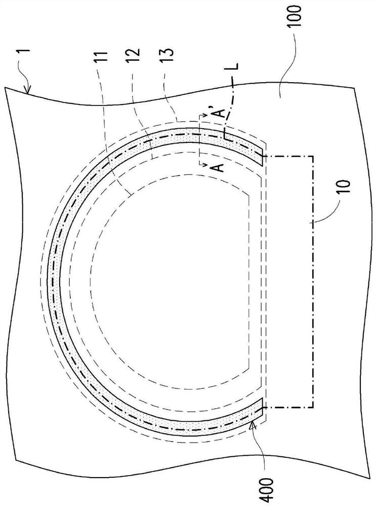
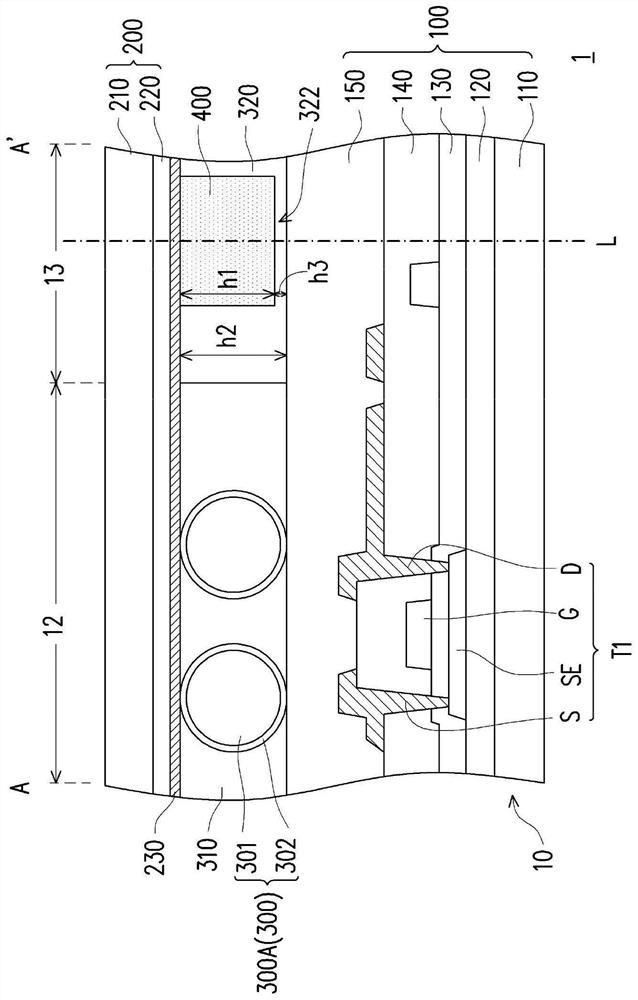
[0060] figure 1 Shown is a top view of a motherboard of an embodiment of the present invention. Please refer to figure 1 , in this embodiment, the motherboard 1 includes a first substrate 100 and a second substrate 200 opposite to the first substrate 100 (shown in figure 2 ), and includes a plurality of panel structures 10 that have been prepared but not yet cut. The uncut panel structure 10 has a display area 11, a first peripheral area 12, a second peripheral area 13 and a cutting line L. Specifically, the motherboard 1 is the first substrate 100 and the second substrate 200 that have not undergone a cutting process. It should be noted that, for the convenience of explanation and observation, figure 1 Omit drawing some components. The following embodiments will take some components disposed on the first substrate 100 as an example, but the present invention is not limited thereto. In other embodiments, figure 1 The components shown can also be disposed on the second s...


PUM

PropertyMeasurementUnit
diameteraaaaaaaaaa
thicknessaaaaaaaaaa

Abstract

A panel structure has a display area, a first peripheral area, and a second peripheral area. The first peripheral area is between the display area and the second peripheral area. The panel structure includes a first substrate, a second substrate opposite to the first substrate, a first sealant, a supporting spacer, and a second sealant. The first sealant is disposed between the first substrate and the second substrate, and is in the first peripheral area. The first sealant includes at least one spacer particle that contacts with the first substrate and the second substrate. The supporting spacer is in the second peripheral area and is disposed on one of the first substrate or the second substrate. A gap is between the supporting spacer and the other one of the first substrate or the second substrate. The second sealant is disposed between the first substrate and the second substrate, and is in the second peripheral area. The second sealant is disposed in the gap.

Description

technical field [0001] The invention relates to a panel, and in particular to a panel structure in which the sealant contacts an auxiliary spacer. Background technique [0002] With the maturity of the mobile device market, display panels have been widely used in various mobile devices, such as tablet computers, smart phones or smart wearable devices, and display panels not only pursue performance, but also continue to move towards thinner and more beautiful Appearance and other directions of development. [0003] In the existing manufacturing methods of display panels, the display panels are easily affected by external moisture in the process of electronic components, such as metal oxide thin film transistors, resulting in electrical abnormalities of electronic components, thereby reducing performance. In addition, during the cutting and separation process, the non-rectangular panel tends to generate stress at the edge of the display panel and cause chipping, which affects...

Claims


Application Information

Patent Timeline
Patent Type & Authority Patents(China)
IPC IPC(8): H01L27/12H01L23/00
CPCH01L23/564H01L27/1222H01L27/1225
Inventor 叶家宏黄美莲黄国有
Owner AU OPTRONICS CORP
Learn More