
Manufacture method for switching tube and array substrate

A manufacturing method and array substrate technology, which are applied in the manufacture of array substrates and the manufacture of switching tubes, can solve problems such as molybdenum metal residues, short circuits, and electrical abnormalities of thin-film transistors, so as to avoid electrical abnormalities, prevent short circuits, and improve the manufacturing process. The effect of yield

Active Publication Date: 2015-06-17
TCL CHINA STAR OPTOELECTRONICS TECH CO LTD
View PDF5 Cites 0 Cited by
  • Summary
  • Abstract
  • Description
  • Claims
  • Application Information

AI Technical Summary

Problems solved by technology

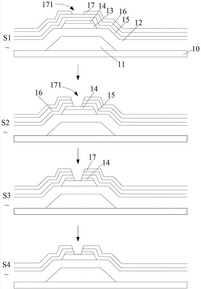
[0005] In the above steps, on the one hand, due to the addition of one layer of molybdenum metal layer 15, on the other hand, it is necessary to use copper etching solution to etch the copper metal layer 16 and molybdenum metal layer 15 in step S2. When the selection of molybdenum is relatively large, it will cause the copper metal layer 161 to be etched to meet the requirements, but the molybdenum metal layer 15 has not been etched completely, so the residue of molybdenum metal will be caused; although fluorine compounds can be added in the etching solution to effectively remove the molybdenum metal, but Fluorine compounds will etch the glass substrate 10, the insulating layer 12, the semiconductor layer 13 and the ohmic contact layer 14, making it impossible to carry out process rework
At the same time, if the molybdenum metal is not removed, the remaining molybdenum metal will affect the process of dry etching the ohmic contact layer 14 in step S3, and the dry etching cannot be carried out smoothly, and finally the remaining molybdenum metal will also lead to the formation of the source electrode. The electrode 162 and the drain electrode 163 are short-circuited, causing the electrical abnormality of the thin film transistor

Method used


Image

  • Manufacture method for switching tube and array substrate
  • Manufacture method for switching tube and array substrate
  • Manufacture method for switching tube and array substrate

Examples


Embodiment Construction

[0019] The present invention will be described in detail below with reference to the drawings and embodiments.

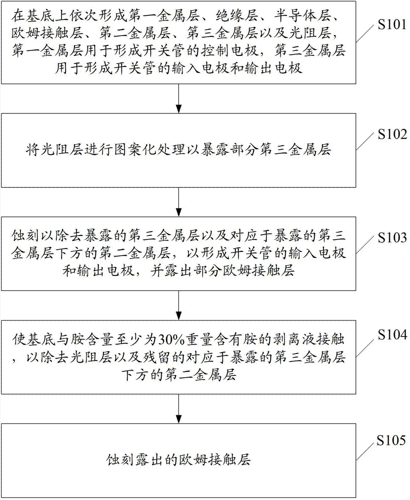
[0020] refer to figure 2 , the present invention is applied to an embodiment of the manufacturing method of the switching tube of the array substrate, including the steps:

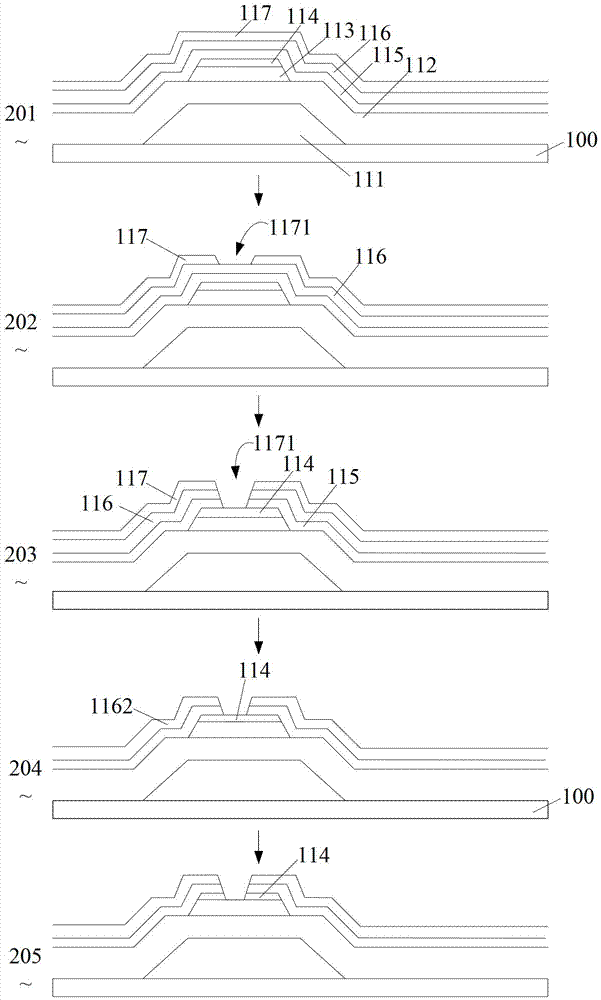
[0021] Step S101: sequentially forming a first metal layer 111, an insulating layer 112, a semiconductor layer 113, an ohmic contact layer 114, a second metal layer 115, a third metal layer 116, and a photoresist layer 117 on the substrate 100, the first metal layer 111 It is used to form the control electrode of the switch transistor, and the third metal layer 116 is used to form the input electrode and the output electrode of the switch transistor.

[0022] The switch tube is a three-terminal control switch. In order to clearly describe the manufacturing process of the switching tube of the present invention, in conjunction with image 3 A schematic diagram of the fabrication process is sh...


PUM


Abstract

A method for manufacturing a switch tube and a method for manufacturing an array substrate, including: firstly forming a first metal layer (111), an insulation layer (112), a semiconductor layer (113), an Ohmic contact layer (114), a second metal layer (115), a third metal layer (116) and a photoresist layer (117) sequentially on a substrate (100); after patterning the photoresist layer (117), etching the third metal layer (116) and the second metal layer (115) to form an input electrode and an output electrode of a switch tube; using a stripping solution with an amine content of at least 30% by weight to remove the photoresist layer (117) and the residual metal; and finally etching the Ohmic contact layer (114). In this way, electrical anomalies in a switch tube can be effectively avoided and the yield of manufacturing procedures can be increased.

Description

technical field [0001] The invention relates to the technical field of liquid crystal production, in particular to a production method of a switch tube and a production method of an array substrate. Background technique [0002] Thin Film Transistor (TFT, Thin Film Transistor) is one of the important elements of the array substrate. The thin film transistor technology is the core of liquid crystal display technology and has a great impact on the quality of liquid crystal display. [0003] In the manufacturing process of thin film transistors, it generally goes through processes such as cleaning, film formation, photolithography, inspection and repair. The core process is photolithography, which mainly includes photoresist coating, exposure, development, etching, and stripping. When fabricating the metal wiring of the thin film transistor on the substrate, since the resistivity of copper is small, it is more suitable for making the metal wire circuit of the large-scale liquid...

Claims


Application Information

Patent Timeline
Patent Type & Authority Patents(China)
IPC IPC(8): H01L21/336H01L21/77
CPCH01L29/458H01L29/66765
Inventor 周佑联陈柏林
Owner TCL CHINA STAR OPTOELECTRONICS TECH CO LTD
Learn More