An organic electroluminescent device and a display device

An electroluminescent device and electroluminescent technology, applied in the direction of electro-solid devices, electrical components, luminescent materials, etc., can solve the problems of low luminous efficiency and low lifespan of devices, and achieve the goal of improving luminous efficiency, reducing energy level barrier, improving Effect of Luminous Efficiency and Lifespan

Inactive Publication Date: 2019-01-25
YUNGU GUAN TECH CO LTD
View PDF6 Cites 7 Cited by
  • Summary
  • Abstract
  • Description
  • Claims
  • Application Information

AI Technical Summary

Problems solved by technology

[0004] However, the use of TADF materials in the light-emitting layer of organic electroluminescent devices often has low luminous efficiency and low lifespan.

Method used


Image

  • An organic electroluminescent device and a display device
  • An organic electroluminescent device and a display device
  • An organic electroluminescent device and a display device

Examples


Embodiment 1-7

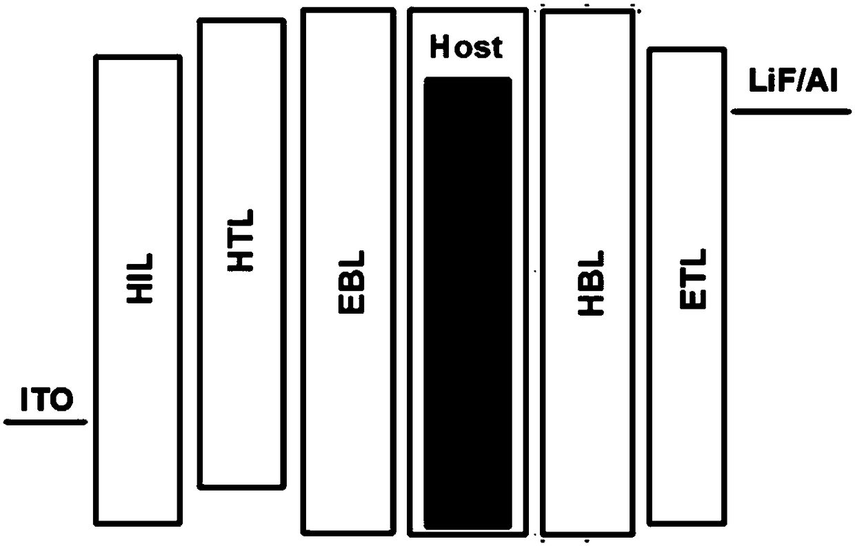
[0057] Embodiments 1-7 respectively provide an organic electroluminescent device, such as figure 2 As shown, the device structure sequentially includes ITO anode, hole injection layer (HIL), hole transport layer (HTL), electron blocking layer (EBL), light emitting layer (EML), hole blocking layer (HBL), electron transport layer layer (ETL), electron injection layer (EIL) and cathode.

[0058] Wherein, the material of the hole injection layer is HATCN, and generally the total thickness is 5-30nm, which is 10nm in this embodiment. The material of the hole transport layer is a common material for HTL in OLEDs, which is NPB in this embodiment, and generally has a total thickness of 5-500 nm, and is 40 nm in this embodiment. The thickness of the electron blocking layer is generally 1-500nm, which is 5nm in this embodiment. The host material (Host) of the light-emitting layer is consistent with the materials of the electron blocking layer and the hole blocking layer, the guest ma...

Embodiment 8-10

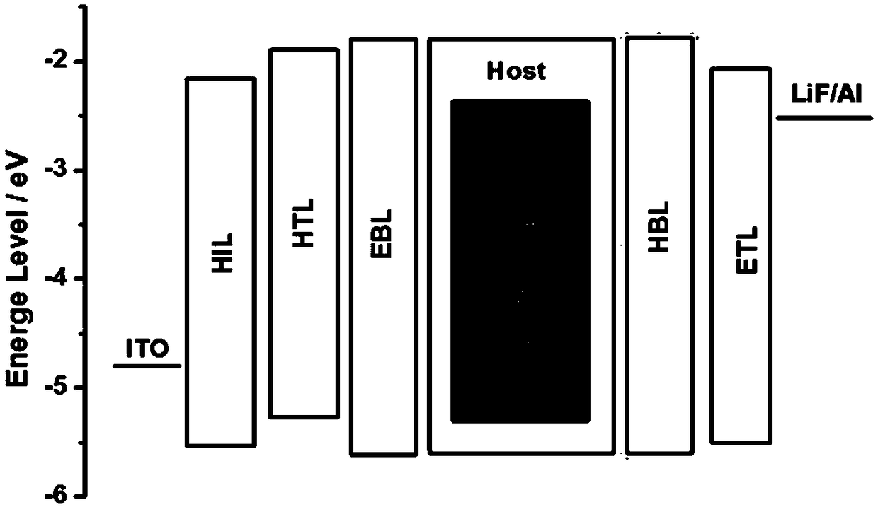
[0077] Embodiments 8-10 respectively provide an organic electroluminescent device, such as image 3 As shown, the device structure sequentially includes ITO anode, hole injection layer (HIL), hole transport layer (HTL), electron blocking layer (EBL), light emitting layer (EML), hole blocking layer (HBL), electron transport layer layer (ETL), electron injection layer (EIL) and cathode. Among them, the host material (Host) of the light-emitting layer, the material of the hole blocking layer and the material of the electron blocking layer are all the same, and the TADF material is used as the sensitizer of the light-emitting layer, and the traditional fluorescent dye is used as the guest material of the light-emitting layer (ie Fluorescent dyes). The materials and thicknesses used for other functional layers are consistent with those in Examples 1-7. The thickness of the light-emitting layer is 30 nm, the thickness of the hole blocking layer is 5 nm, and the thickness of the ele...

Embodiment 1

[0090] Embodiments 11-14 respectively provide an organic electroluminescent device, the structure of which is consistent with that of Embodiments 1-7. For details, please refer to figure 2 . The material and thickness used for each functional layer of the OLED device in Examples 11-14 are basically the same as those in Example 1, the only difference lies in the thickness of the electron blocking layer and the hole blocking layer.


PUM

PropertyMeasurementUnit
thicknessaaaaaaaaaa
thicknessaaaaaaaaaa
thicknessaaaaaaaaaa

Abstract

The invention provides an organic electroluminescent device and a display device, wherein the organic electroluminescent device comprises a light emitting layer, a hole blocking layer and an electronblocking layer, wherein the material of the light emitting layer comprises a host material; The materials of the hole barrier and electron barrier are the same as the host materials. An organic electroluminescent device, Using the same material as the main material of the light-emitting layer, hole blocking layer and electron blocking layer, can effectively reduce the energy level barrier betweenthe main body of the light-emitting layer and the adjacent hole blocking layer and electron blocking layer, reduce the device turn-on voltage, improve the light-emitting efficiency, and also prolong the service life of the device.

Description

technical field [0001] The invention belongs to the field of display technology, and in particular relates to an organic electroluminescent device and a display device. Background technique [0002] Organic electroluminescent devices are provided with a light-emitting layer between the electron-transporting layer and the hole-transporting layer, and a cathode and an anode are further arranged outside it, and electrons and holes are injected into the device by an external voltage and recombine in the light-emitting layer to form an excitation layer. A photon, a device that emits photons and deactivates them through the process of fluorescence or phosphorescence. Because of its full solid state, self-illumination, wide viewing angle, fast response, low driving voltage, low energy consumption and many other characteristics, it has great application prospects in the field of display and lighting. [0003] In recent years, a new generation of thermally activated delayed fluoresc...

Claims


Application Information

Patent Timeline
Patent Type & Authority Applications(China)
IPC IPC(8): H01L51/50H01L51/54H01L27/32C07C211/61C07C211/58C07D271/107C07D209/86C07D251/24C07F7/08C07D239/26C07F9/50C07C43/205C07C15/56C09K11/06
CPCC09K11/06C07C15/56C07C43/2055C07C211/58C07C211/61C07D209/86C07D239/26C07D251/24C07D271/107C07F7/0807C07F9/5022C09K2211/1096C09K2211/1059C09K2211/1048C09K2211/1044C09K2211/1029C09K2211/1014C09K2211/1011C09K2211/1007H10K59/00H10K85/615H10K85/624H10K85/631H10K85/626H10K85/633H10K85/654H10K85/6565H10K85/40H10K85/6572H10K50/121H10K50/12H10K50/18H10K50/11
Inventor 李国孟魏金贝李梦真李维维何麟
Owner YUNGU GUAN TECH CO LTD
Why Eureka
Try Eureka