An organic electroluminescent device and a display device
An electroluminescent device and electroluminescent technology, which are applied in the direction of electro-solid devices, electrical components, semiconductor devices, etc., can solve the problems of low luminous efficiency and low life of the device, and improve the luminous efficiency, reduce the energy level barrier, reduce the The effect of turn-on voltage
- Summary
- Abstract
- Description
- Claims
- Application Information
AI Technical Summary
Problems solved by technology
Method used
Image
Examples
Embodiment 1-8
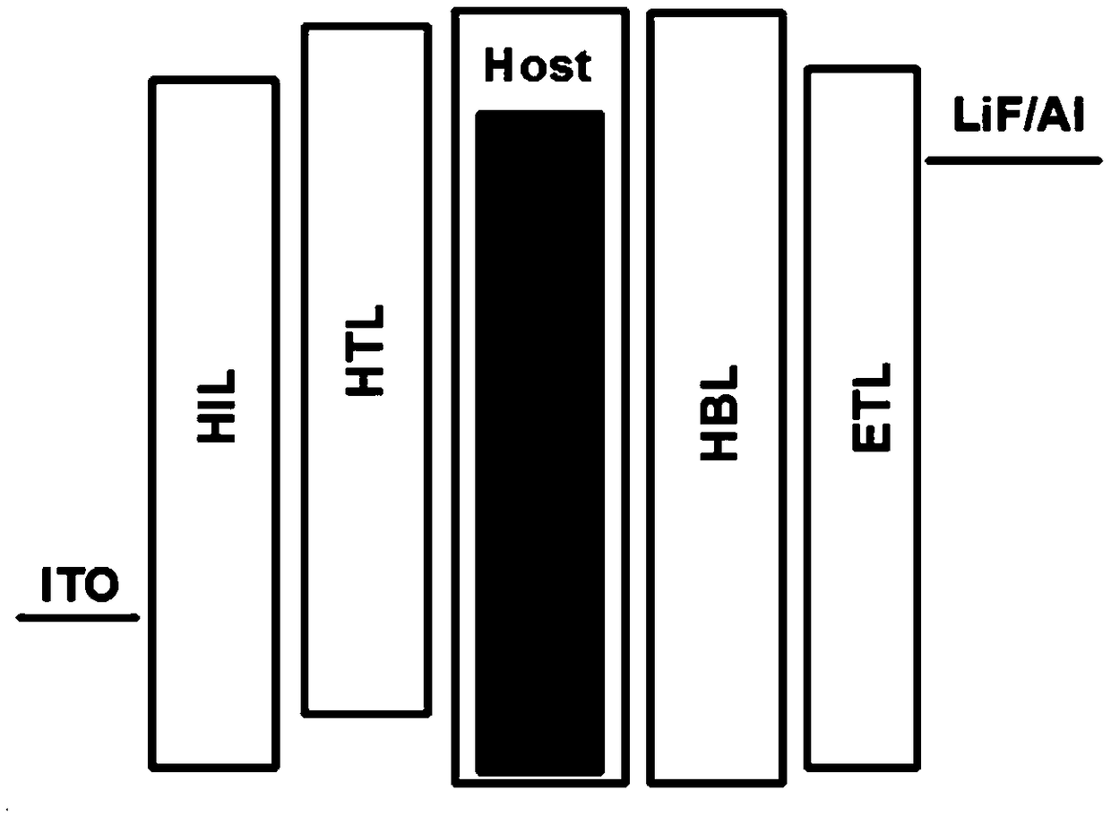
[0056] Embodiments 1-8 respectively provide an organic electroluminescent device, such as figure 2 As shown, the device structure includes ITO anode, hole injection layer (HIL), hole transport layer (HTL), light emitting layer (EML), hole blocking layer (HBL), electron transport layer (ETL), electron injection Layer (EIL) and cathode.
[0057] Wherein, the material of the hole injection layer is HATCN, and the total thickness is generally 5-30 nm, which is 10 nm in this embodiment. The material of the hole transport layer is a commonly used material for HTL in OLED. In this embodiment, it is NPB, and the total thickness is generally 5-500 nm. In this embodiment, it is 40 nm. The host material of the light-emitting layer is the same as the material of the hole blocking layer, the guest material is TADF material (TADFEmitter), and the doping concentration is 0.1-50wt%; the thickness of the light-emitting layer is generally 1-200nm, in this embodiment it is 30nm . The thickness o...
Embodiment 9-14
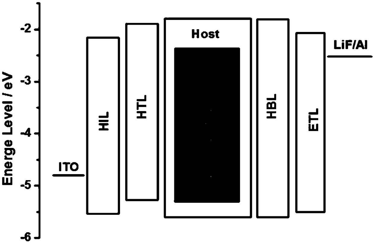
[0073] Examples 9-14 respectively provide an organic electroluminescent device, such as image 3 As shown, the device structure includes ITO anode, hole injection layer (HIL), hole transport layer (HTL), light emitting layer (EML), hole blocking layer (HBL), electron transport layer (ETL), electron injection Layer (EIL) and cathode. Among them, the host material (Host) of the light-emitting layer is the same as the material of the hole blocking layer, and TADF material is used as the sensitizer of the light-emitting layer, and traditional fluorescent dyes are used as the guest material of the light-emitting layer (ie, Fluorescentdyes). The materials and thicknesses of the other functional layers are the same as in Examples 1-8, the thickness of the light-emitting layer is 30 nm, and the thickness of the hole blocking layer is 5 nm.
[0074] See Table 2 for specific material selection, doping concentration, and performance test results of the OLED device in the corresponding embod...
Embodiment 15-18
[0084] Examples 15-18 respectively provide an organic electroluminescent device, the device structure of which is the same as that of Examples 1-8. For details, please refer to figure 2 . The materials and thicknesses of the functional layers of the OLED devices in Examples 15-18 are basically the same as those in Example 2, except for the thickness of the hole blocking layer. The thickness of the hole blocking layer in Examples 15-18 is 1 nm, 10 nm, 50 nm, and 100 nm, respectively, and the performance test results of the corresponding OLED devices are shown in Table 3.
[0085] table 3
[0086]
[0087] It can be seen from Table 3 that when the host material of the light-emitting layer is consistent with the material of the hole blocking layer, as the thickness of the hole blocking layer changes, the luminous efficiency and lifetime of the organic electroluminescent device change. According to the test results of Examples 15-18 and the foregoing Examples 1-14, when the thickness...
PUM
 Abstract
Description
Claims
Application Information


